
Index 368
Negative oxygen ion generator 1
Published:2011/6/27 23:00:00 Author:Nicole | Keyword: oxygen ion, generator
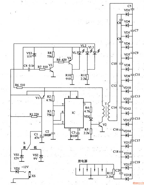
This negative oxygen ion generator circuit is composed of power supply steady voltage circuit, under voltage detection indication circuit, high frequency oscillator and high voltage generator circuit, it is shown in the figure 9-113.
The power supply steady voltage circuit is made of diode VD1, power supply regulator V1, steady voltage diodes VS1, VS2, ionization selection switch S, power supply indication LED VL2 and peripheral resistor capacitor components.
The under voltage detection indication circuit consists of transistors V3, V4, steady voltage diode VS3, under voltage indication LED VL1 and peripheral resistor capacitor components.
(View)
View full Circuit Diagram | Comments | Reading(4942)
Wireless remote control electric initiator 2
Published:2011/6/30 22:26:00 Author:Nicole | Keyword: wireless remote control, electric initiator
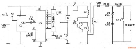
The wireless receive initiation circuit is composed of power switch S2(S2-1, S2-2), battery GB2, receiving antenna A2, wireless receive integrated circuit IC3, wireless decoding integrated circuit IC4, resistors R2-R6, capacitors C3-C5, transistors V1, V2, diodes VD1, VD2, relay K and boost transformer T, it is shown in the figure 8-28. The wireless receive control circuit is made of A2, IC3, IC4, C3, R2, R3, VDl, Vl and K, the oscillation boost circuit consists of R4, V2, T, the charge-discharge circuit is composed of VD2, R5, C4, C5, R6.
(View)
View full Circuit Diagram | Comments | Reading(454)
Electric welding machine no load electricity saver 3
Published:2011/6/30 20:30:00 Author:Nicole | Keyword: electric welding machine, electricity saver
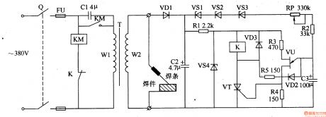
The electric welding machine no load electricity saver circuit is composed of power supply circuit, delay trigger circuit and control implement circuit, it is shown in the figure 8-7.
The power supply circuit is made of knife switch Q, fuse FU, the normally open contact of AC contactor KM, electric welding machine transformer T, rectifier diode VD1, filter capacitor C2, steady voltage diode VS1 and current limiting resistor R1.
The delay trigger circuit consists of steady voltage diode VS2, VS3, potentiometer RP, resistors R2-R5, capacitor C3, diode VD2 and unijunction transistor VU.
(View)
View full Circuit Diagram | Comments | Reading(2360)
Electric welding machine no load electricity saver 2
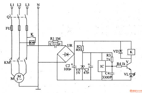
Published:2011/6/30 20:23:00 Author:Nicole | Keyword: electric welding machine, electricity saver
The electric welding machine no load electricity saver circuit is composed of power supply circuit, pulse oscillator, monostable trigger and control circuit, it is shown in the figure 8-6.
The power supply circuit is made of depressurization capacitor C1, resistor R1, steady voltage diode VS1, rectifier diode VD2 and filter capacitor C2.
The pulse oscillator consists of time base integrated circuit IC1 and peripheral devices.
The monostable trigger is composed of time base integrated circuit IC2 and resistor R5, capacitor C5.
The control circuit is made of optical coupler VLC, relay K, AC contactor KM and TRIAC VT.
(View)
View full Circuit Diagram | Comments | Reading(3418)
Electric welding machine no load electricity saver 1
Published:2011/6/30 20:15:00 Author:Nicole | Keyword: electric welding machine, electricity saver
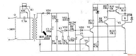
The electric welding machine no load electricity saver circuit is composed of relay drive circuit, low voltage detection control circuit, high voltage timing control circuit or voltage self-adaptive tracking regulation circuit, it is shown in the figure 8-5.
The low voltage detection control circuit is made of relay K's normally closed contact K2, steady voltage diode VS1, resistor R1 or transistor V6.
The high voltage timing control circuit consists of steady voltage diode VS2, resistors R2, R6, capacitor C2 or transistor V5.
The relay drive circuit is composed of relay K, transistors V1, V2 and diode VD3.
(View)
View full Circuit Diagram | Comments | Reading(2979)
8-gear constant-current current design the circuit diagram
Published:2011/5/13 4:02:00 Author:Ecco | Keyword: 8-gear, constant-current , current design
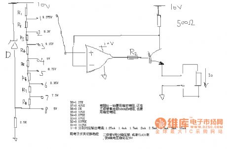
Resistors R1-R8 use precision resistors, the 500R resistors of the transistor collector also use precision resistors. Electronic switch can change the gears, the diode D uses a 5V regulator, or TL431 to make the D terminal voltage be stable at 5V.Resistors R1-R8 use precision resistors, the 500R resistors of the transistor collector also use precision resistors. Electronic switch can change the gears, the diode D uses a 5V regulator, or TL431 to make the D terminal voltage be stable at 5V.
(View)
View full Circuit Diagram | Comments | Reading(487)
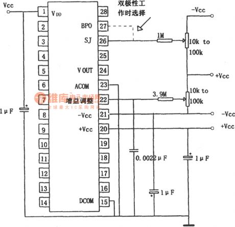
The dual-channel dual-power isolation in-phase gain circuit diagram composed of 3656
Published:2011/5/17 3:14:00 Author:Ecco | Keyword: dual-channel , dual-power , isolation , in-phase gain
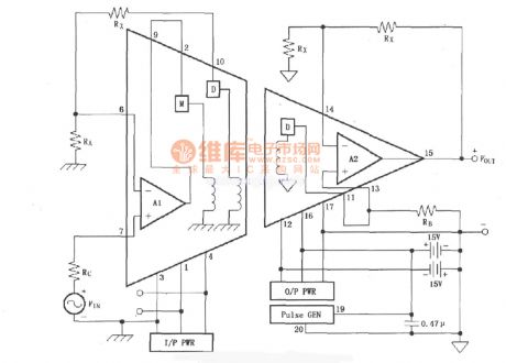
The dual-channel dual-power isolation in-phase gain circuit diagem composed of 3656 is shown as the chart. There is a bipolar power supply composed of two 15V powers being added to the pin 12,16, they have common ground which is the the ground of output level (pin 17 ), one of the two power supplies (+ V) is used as power supply for pulse generator (pin 19,20 ). Pin 12,16 do not need increase filter capacitor. The voltage isolation of the circuit: there is 3500V between the pin 3 and pin 17, pin 3 and pin 19, no voltage isolation between the pin 17 and pin 19.
(View)
View full Circuit Diagram | Comments | Reading(371)
Two-channel single-supply inverting gain circuit diagram composed of 3656
Published:2011/5/13 4:02:00 Author:Ecco | Keyword: Two-channel, single-supply , inverting gain
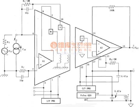
Two-channel single-supply inverting gain circuit diagram composed of 3656 is shown as the chart. The system uses a power supply to constitute an unipolar power supply circuit, the power ground is connected to output level ground (pin 17) to provide internal generating power for the other polarity power supply of A2, so filter is added to the pin 12. The isolated power supply can also be used for the input stage. The voltage isolation of the structure circuit: there is 3500V between the pin 3 and pin 17, pin 3 and pin 19, no isolation between the pin 19 and pin 17.
(View)
View full Circuit Diagram | Comments | Reading(442)
Bipolar noise treatment method circuit diagram composed of ISO100
Published:2011/5/17 3:29:00 Author:Ecco | Keyword: Bipolar, noise treatment method
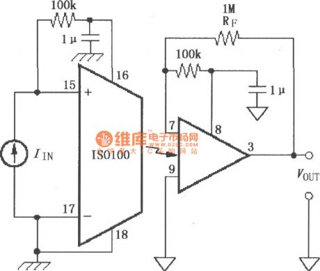
Bipolar noise treatment method circuit diagram composed of ISO100 is shown as the chart. In bipolar mode, the noise is primarily produced by the reference current source. The reference current source is added a low-pass filter to reduce the noise of the current source.
(View)
View full Circuit Diagram | Comments | Reading(392)
The monitoring (ISO122P/124, INA105) circuit diagram of battery system
Published:2011/5/17 3:23:00 Author:Ecco | Keyword: monitoring , battery system
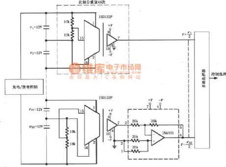
The 600V monitoring (ISO122P/124, INA105) circuit diagram of battery system composed of ISO122P/124 and instrumentation amplifier INA105, multi-route selector is shown as the chart. Circuit can detect the charging and discharging 50 pieces of 12V batteries connected in series ( the total voltage is 600V) to prevent over charge or over discharge. The input voltage of ISO122P/124 is e / 2 voltage got by the two ends of a single 12V battery divided by two 10kΩ, and it is isolated, amplified and sent to INA105. INA105 is connected as an inverting amplifier gain, it outputs e / 2 to the multiplexer, the multiplexer would controll the selection of output.
(View)
View full Circuit Diagram | Comments | Reading(449)
Capacitive dimmer switch circuit (1)
Published:2011/6/28 2:36:00 Author:Ecco | Keyword: Capacitive , dimmer switch
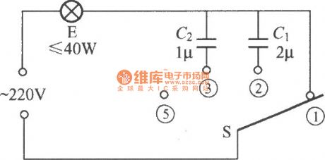
Capacitive dimmer switch circuit is shown as the chart, it uses the principle of capacitors having AC capacitance. When S is located in the position in the figure, E bulb emits normal light, that is the maximum brightness; when it is switched to the position ②, as the 2μF capacitor is connected in series C1, light intensity of E decreases; when it is switched to the position ③, because of C2
(View)
View full Circuit Diagram | Comments | Reading(798)
Capacitive dimmer switch circuit (2)
Published:2011/6/28 2:35:00 Author:Ecco | Keyword: Capacitive , dimmer switch
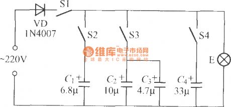
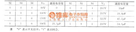
The circuit described as the chart is the dimmer switch circuit which uses the capacitor discharging principle, and it is suitable for incandescent light, and it has no interference effect on radio, television and other appliances. The principle of the circuit is shown as the chart. The relationship of voltage VE across the lamp and the switch combination is shown as the following table:
(View)
View full Circuit Diagram | Comments | Reading(528)
Electric sewing machine no load energy saver 2
Published:2011/6/30 0:49:00 Author:Nicole | Keyword: sewing machine, no load energy saver
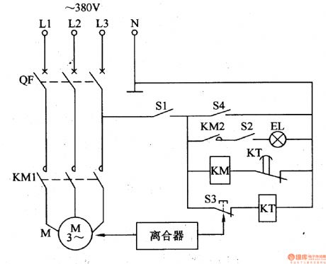
The electric sewing machine no load energy saver circuit is composed of low high circuit breaker QF, control switch S1, light switch S2, S4, footage switch S3, AC contactor KM and time relay KT, it is shown in the figure 8-4.
When it is used, the low high circuit breaker QF is turned on, then S1, S2 are turned on, the sewing worker puts her feet on the clutch pedal, the foot switch S3 is cut off, KM pulls in, its normally open contact KM1 is connected, the motor M starts running, light EL turns on, the work can start to sew.
(View)
View full Circuit Diagram | Comments | Reading(600)
Electric sewing machine no load energy saver 1
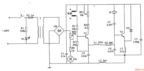
Published:2011/6/29 23:02:00 Author:Nicole | Keyword: sewing machine, no load energy saver
The electric sewing machine no load energy saver circuit is composed of DC regulated power supply circuit, sensor control circuit and master control circuit, it is shown in the figure 8-3.
The DC regulated power supply circuit is made of hypotension capacitor C1, discharge resistor R1, bridge rectifiers UR, filter capacitor C2, C3, current limiting resistor R2 and steady voltage diode VS.
The sensor control circuit consists of magnet which is fixed on the sewing machine clutch operating lever and Hall sensor integrated circuit IC, resistors R3, R4, capacitor C4, transistor V, diode VD, LED VL and relay K.
(View)
View full Circuit Diagram | Comments | Reading(2230)
Medical ultrasonic atomizer 3
Published:2011/6/29 22:48:00 Author:Nicole | Keyword: ultrasonic atomizer
The medical ultrasonic atomizer circuit is composed of power supply circuit, on the low side of liquid level protection control circuit, ultrasonic oscillator and fan drive circuit, it is shown in the figure 9-112.
The power supply circuit is made of power supply switch S, resistor R1, power supply indication LED VL, fuse FU, power transformer T, bridge rectifiers UR and filter capacitor C1.
The low side of liquid level protection control circuit consists of liquid level detection electrodes a, b, resistors R2-R4, potentiometer RP1, potentiometer C2 and transistor V1.
(View)
View full Circuit Diagram | Comments | Reading(4207)
Photoelectric shooting automatic acousto-optic target-reporting circuit diagram
Published:2011/6/24 1:27:00 Author:Nicole | Keyword: photoelectric shooting, acousto-optic target-reporting
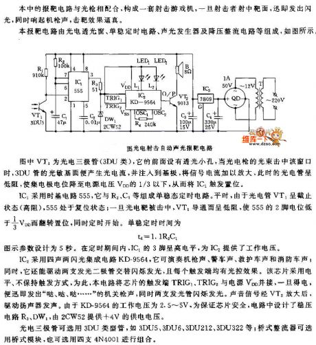
In the figure, VT1 is photoelectric triode(3DU type), there is a light hole in front of it, when the photoelectric gun's light beam hits this window, 3DU tube's photosensitive base surface will produce photocurrent, and it is injected into the base collector, the signal current is amplified, then the photoelectric tube is low resistance, the collector level is dropped below 1/3 power supply VDD, IC1 is triggered and set.
IC1 adopts time base circuit 555, the monostable timing circuit is composed of IC1 and R2, C1. Ordinarily, photoelectric tube VT1 is in off state(high resistance), 555 is in reset state; once the photoelectric target is hit, VT1 is turned on and it is low resistance, 555's 2 foot level is lower than 1/3 VDD, it is reversed and set, at the same time, the timing starts. The monostable timing time is td=1.1R2C1.
(View)
View full Circuit Diagram | Comments | Reading(416)
The hit automatic acousto-optic target-reporting circuit diagram(1)
Published:2011/6/24 1:42:00 Author:Nicole | Keyword: acousto-optic target-reporting
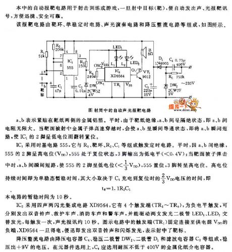
This target-reporting circuit is composed of target ring, monostable timing circuit, acousto-optic performance circuit and depressurization rectifier circuit, the figure is as shown.
IC1 adopts time base circuit 555, the trigger timing circuit is composed of IC1 and R1, target ring, R2, C1. Ordinarily, a and b are insulated, 555's 2 foot is high level(VDD), 555 is in reset state, 3 foot output is low level(<0.4V); when the target surface is hit by bullet, a, b are short circuit instantaneous, 555's 2 foot is low level(<1/3 VDD), 555 is set, 3 foot turns to high level. The high level duration time is the monostable temporary stability time, it is decided by the 2/3 VDD voltage time of C1 charges to reset, namely, td=1.1R2C1, the temporary stability time is 10s.
(View)
View full Circuit Diagram | Comments | Reading(400)
Preventing goods from being forgotten reminding circuit diagram
Published:2011/6/24 2:02:00 Author:Nicole | Keyword: goods, reminding
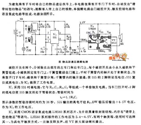
It has two magnetic control switches, they are fixed in the left and right car doors of taxi. Each magnetic control switch is composed of small permanent magnet and reed switch, the small magnet is fixed in the car door, the reed switch is set in the door head, ordinarily, the contact piece inside the reed switch is always in off state. When the passenger gets off, the magnet and reed switch are separated, the contact piece is turned on, 555's 2 foot turns to low level, 555 is set to high level, it provides IC2 with power supply.
IC1 adopts 555 time base circuit, the monostable trigger circuit is composed of IC1 and R2, C1, R3, C3. When the car door is open, 555 is tirggered by 2 foot's low level and it is in triplet state, the temporary stability time is td=1.1R2C1.
(View)
View full Circuit Diagram | Comments | Reading(417)
Infrared reflection car space reminding circuit diagram
Published:2011/6/24 3:53:00 Author:Nicole | Keyword: Infrared reflection, car space, reminding
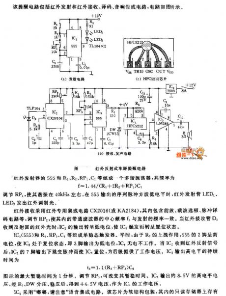
A multivibrator is composed of infrared transmitter's 555 and R1, R2, RP1, C1, the frequency is f=1.44/(R1+2R2+RP1)C1. The resonance can be about 40kHz by adjusting RP1, when the sequence pulse square wave which is outputed by 555 is low level, infrared launch tube LED1, LED2 emits infrared modulated light.
The infrared receiving adopts infrared special integrated circuit CX2016(or KA2184), it contains preamplifier, carrier frequency selection, pulse decoding circuit, the internal bandpass filter's center frequency f0 is coincidence with transmitting frequency. When the infrared launch tube D3 receives the reflected infrared light, IC2's output turns to low level, IC3 is triggered, and it turns to set state.
(View)
View full Circuit Diagram | Comments | Reading(427)
DAC811 external connection circuit
Published:2011/7/12 1:49:00 Author:zj | Keyword: external, connection circuit
View full Circuit Diagram | Comments | Reading(458)
| Pages:368/471 At 20361362363364365366367368369370371372373374375376377378379380Under 20 |
Circuit Categories
power supply circuit
Amplifier Circuit
Basic Circuit
LED and Light Circuit
Sensor Circuit
Signal Processing
Electrical Equipment Circuit
Control Circuit
Remote Control Circuit
A/D-D/A Converter Circuit
Audio Circuit
Measuring and Test Circuit
Communication Circuit
Computer-Related Circuit
555 Circuit
Automotive Circuit
Repairing Circuit