
Index 369
Color TV pincushion correction circuit diagram 3
Published:2011/6/24 1:45:00 Author:Ecco | Keyword: Color TV , pincushion correction
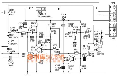
The same circuits with Toshiba 2500XH pincushion correction circuit are as follow: Toshiba 2506XH, 2800XH, 2806XH etc. The field sawtooth voltage is sent to the B pole of QD03 by PD02 (3) feet, RD17, CD14, RD16, RD19, CD10. QD04 is 50Hz/60Hz switch. When the electronic switch is at 50Hz, QD04 ends, and at 60Hz, QD04 is conduction, RD19 is short, sawtooth amplitude sent to QD03B increases. QD03 is parabolic wave voltage generating tube, which can generate the concave parabolic wave voltage at C-pole output, then it is adjusted by the RD51 margin and added to the B pole of QD02, and QD02, QD01 are the parabolic wave amplifier tubes, RD50 is the line width adjustment potentiometer. (View)
View full Circuit Diagram | Comments | Reading(2189)
Color TV pincushion correction circuit diagram 4
Published:2011/6/24 1:49:00 Author:Ecco | Keyword: Color TV, pincushion correction
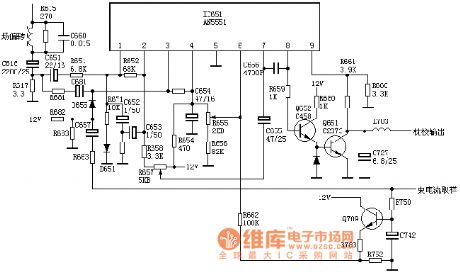
The same circuits with Hitachi CMT2988 pincushion correction circuit are as follow: Hitachi 25M8C, CMT2518, CMT2718, CMT2916, CMT2588, CMT2598, CMT2998, Furi HFC2581, 2586,2587,2986,2987 and so on. The approximately 4V (peak - peak) sawtooth voltage on two ends of R617 is added to the IC651's (1) foot by the C651, R651, then it will be made internal amplification, integration process, pin 2 will out about 2V (peak - peak) concave parabolic wave voltage. R655 is the line width adjustment potentiometer, and R657 is the school pincushion correction adjust potentiometer.
(View)
View full Circuit Diagram | Comments | Reading(1755)
Color TV pincushion correction circuit diagram 5
Published:2011/6/23 22:26:00 Author:Ecco | Keyword: Color TV , pincushion correction
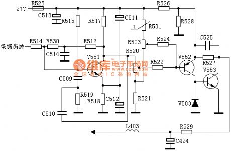
Field sawtooth wave signal is sent to the the V551's base of R514, integrated by the R516, C514, differentiated by E-B pole of C510, R519, C509, V551 to generate parabolic wave signal, and then amplified signal by V552 will be output from the collector, and directly sent to the base of V553. The parabolic wave signal output by from V553 collector is added to the negative side of V402 by R529, L403, then the V401 modulates the line deflection coil current, then the East / West pincushion distortion is corrected. The signal added on the R520 is the parabolic wave signal, and adjusting R520 can change parabolic wave signal amplitude, thus regulate the amount of the pincushion correction.
(View)
View full Circuit Diagram | Comments | Reading(1010)
Color TV pincushion correction circuit diagram 6
Published:2011/6/23 22:09:00 Author:Ecco | Keyword: Color TV , pincushion correction

The circuit is the pincushion correction circuit taken from the Venus D2918 model, and comparing with the pincushion correction circuit -1, it only has more than V951, V950 two stage amplifier, and the reason is that field sawtooth is not from sampling resistor of taken from field deflection coil but the pin of TDA8838's (46). Due to it has a lesser extent, it adds two stage amplifier.
(View)
View full Circuit Diagram | Comments | Reading(1240)
Color TV pincushion correction circuit diagram 8
Published:2011/6/23 21:26:00 Author:Ecco | Keyword: Color TV , pincushion correction
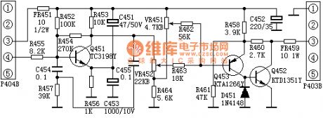
The models using pincushion correction circuit are: Samsung MC-15 movement, Venus C6418, V6458, peony 64C1, Leroy CT6388W and so on. The field sawtooth voltage is sent to pincushion correction circuit through P404 (4) feet, and R455, C454, R457 form the integral circuit to generate integration on field sawtooth wave, then it forms the convex parabolic wave voltage to add to the B pole of parabolic-wave shaping amplifier tube Q451, by the amplification, shaping the output from the C-pole 9V (peak - peak) of the concave parabolic wave voltage, and then by VR451, VR452, R464, R463, R462 component level adjustments, added to the Q453, Q452 composite pipe B-polar. VR451 is the line width adjustment potentiometer, and VR452 is a pincushion adjust potentiometer.
(View)
View full Circuit Diagram | Comments | Reading(755)
SS-D2 red light medical instrument principle and maintenance circuit diagram
Published:2011/6/27 1:35:00 Author:Ecco | Keyword: red light , medical instrument , principle , maintenance
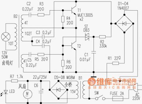
The instrument has two sets of rectifier circuit. One group is AC220V which is limited by R1, bridge rectified by D1 ~ D4, charged on C1 through R2, and when the voltage across C1 is more than turning voltage of two-way trigger diode ST, ST is conduction, so the T2 is first turned on. The coupling effect of winding B2 connected to C2, C5 in series will make T2 turn off, T1 turn on. This will enable the T1 and T2 alternately turn to build high-frequency oscillations.
(View)
View full Circuit Diagram | Comments | Reading(568)
The wiring diagram of measuring three-phase reactive power with a single-phase meter
Published:2011/6/27 1:47:00 Author:Ecco | Keyword: wiring diagram , measuring, three-phase, reactive power , single-phase meter
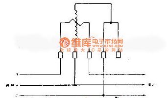
In the case of three-phase symmetric load, the wiring method in the diagram can be used to measure three-phase reactive power. Meter reading multiplied by radical sign of 3 is the three-phase reactive power.
(View)
View full Circuit Diagram | Comments | Reading(761)
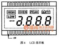
Multi-function digital multimeter TC821 integrated circuit diagram
Published:2011/6/27 1:23:00 Author:Ecco | Keyword: Multi-function , digital multimeter , integrated circuit
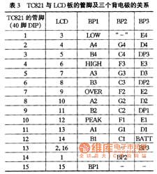
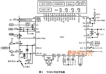
3.1 TC821 main parameters are as follows: ● Supply voltage (V + S connected to the ground) is 15V; ● power consumption is 800mW; ● Operating temperature range: -40 ~ +85 ℃ (D type). 3.2 TC821 main characteristics are as follows: ● The output is displayed as ± 000 when input is zero; ● flip error is ± 1 digit; ● nonlinearity is ± 1 word; ● common mode rejection ratio is 50μV / V; ● noise voltage is 15μV (typical); ● maximum scale factor temperature coefficient is 5ppm / ℃; ● operating current is 1 ~ 1.5mA; ● The maximum adding of input logic low level is 1.5V; ● The minimum decreasing of input logic high level is 1.5V.
(View)
View full Circuit Diagram | Comments | Reading(3618)
Color TV pincushion correction circuit diagram 2
Published:2011/6/24 1:38:00 Author:Ecco | Keyword: Color TV , pincushion correction
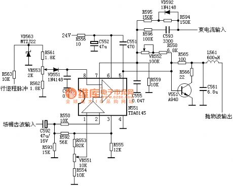
Field sawtooth wave signal is sent to the N551's (2) feet by the C592, R550, then the signal becomes convex parabolic wave voltage on the pin 7 after limited, amplified, waveform processed by IC, at the same time, the voltage added to an internal inverting op amp input and 8-pin input line frequency sawtooth is operated and approved to drive the pin 5 of to output, then it forms the concave parabolic wave field voltage (amplitude is controlled by the parabolic wave field frequency modulation of the line voltage pulse). This voltage amplified by V551, then the L561 output field parabolic wave voltage.
(View)
View full Circuit Diagram | Comments | Reading(1236)
The internal block circuit diagram of LA5521 IC
Published:2011/6/23 2:44:00 Author:Ecco | Keyword: internal block , IC
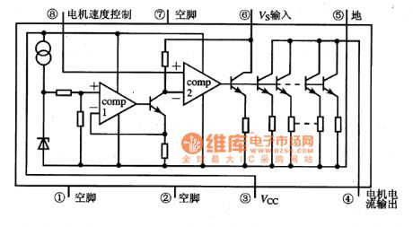
The features of functionsLA5521 IC includes voltage reference circuit, the motor speed control circuit, differential amplifier circuit and other ancillary circuitry. The block diagram of the circuit is shown as the chart.
(View)
View full Circuit Diagram | Comments | Reading(546)
74 series digital circuit 74LS447, BCD seven sections decoder/driver
Published:2011/6/26 21:12:00 Author:Nicole | Keyword: 74 series, digital circuit, decoder, driver
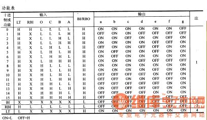
74LS447, BCD-seven sections decoder/driver
It is 74LS447's voltage form, the withstand voltage is 7V; the collector open circuit directly drives indicator; it has a test light; front/back edge cuts off 0 ; the brightness of indicator can be adjusted, the pin and functional table are the same as 74LS447.
(View)
View full Circuit Diagram | Comments | Reading(950)
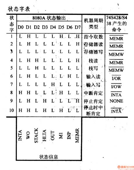
74 series digital circuit 74S428 system controller and bus driver
Published:2011/6/26 21:52:00 Author:Nicole | Keyword: 74 series, digital circuit, system controller, bus driver
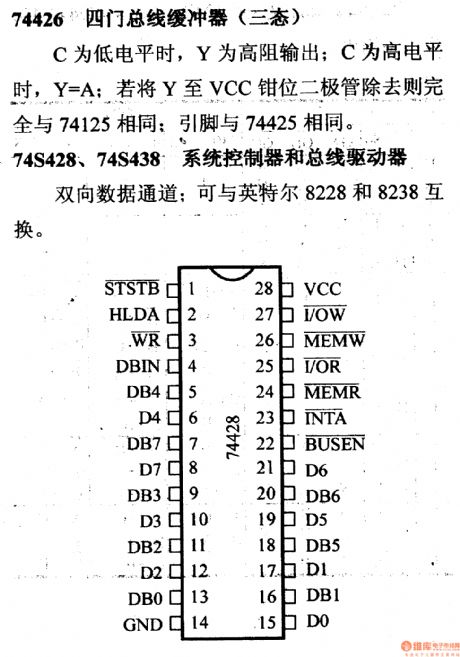
74426 four gates bus buffer(there states)
C is low level, Y is high resistance output; when C is high level, Y=A, if the diodes of Y to VCC clamped are removed, then it is the same as 74125 absolutely; the pin is the same as 74425.
74S428, 74S438 system controller and bus driver
two-way data channel: it can be exchanged with Intel 8228 and 8238.
(View)
View full Circuit Diagram | Comments | Reading(786)
The typical application circuit of nRF401 single RF transceiver
Published:2011/6/23 2:55:00 Author:Ecco | Keyword: typical application circuit , single RF transceiver
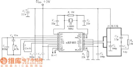
nRF401 typical application circuit is shown in the figure, UDD uses +3 V power supply. The R1, JT, C1 and C2 constitute the crystal oscillator circuit, C3, C4 and R2 form the loop filter. R3 is the power setting resistor. C5 is decoupling capacitors for power, C6 and C7 are de-noising capacitors. DIN, DOUT terminals are respectively connected to Microcontroller TXD (serial output), RXD (serial input) side. For simplifying the circuit, nRF401 and μC can be combined with a crystal oscillator circuit, the circuit is shown as below. X1, X2 are the crystal μC input and output, the oscillator frequency is directly added to the nRF401 end of XC2.
(View)
View full Circuit Diagram | Comments | Reading(464)
The internal block circuit diagram of LA4505 IC
Published:2011/6/23 2:54:00 Author:Ecco | Keyword: internal block , IC
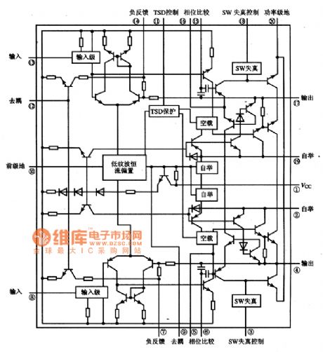
LA4505 IC contains a pair of preamp with input level, low ripple constant current bias, over-temperature protection (TSD), audio mute, popping sound suppression, the load-load protection, bootstrap and distortion switch control circuit. The block diagram of the circuit is shown as the chart.
The internal block circuit diagram of LA4505 IC is shown as the chart.
(View)
View full Circuit Diagram | Comments | Reading(1484)
TDA9373 Multi-functional super monolithic IC diagram
Published:2011/6/23 2:51:00 Author:Ecco | Keyword: Multi-functional , super , monolithic, IC
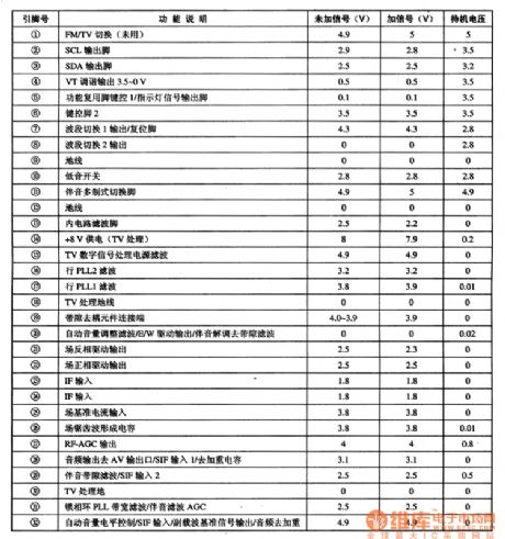
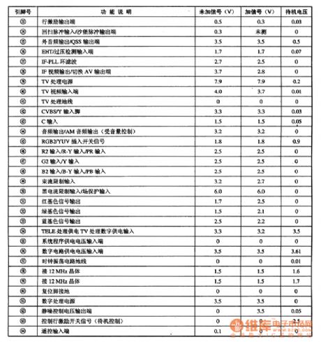
TDA9373 is a multi-functional super monolithic integrated circuit produced by Philips, it is widely used in domestic and imported large screen color television sets, such as Changhong, TCL, Konka, Hisense and so on. 1. Features of functionTDA9373 integrated circuit contains micro-control processor, TV signal processing circuit, the character display control circuit, and horizontal and vertical geometry correction circuit and some other subsidiaries. 2. Pin functions and data TDA9373 IC uses 64-pin double rows package, the pin function and the data are shown in Table 1. Table 1 shows TDA9373 integrated circuit pin functions and data.
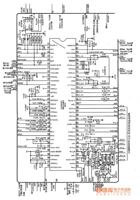
3. Typical application circuit The TV signal processing and control typical application circuit composed of TDA9373 Integrated Circuit is shown in Figure 1, which is the applicating way of CH-16 five-way Changhong color TV. Figure 1 shows TDA9373 IC typical application circuit.
(View)
View full Circuit Diagram | Comments | Reading(3303)
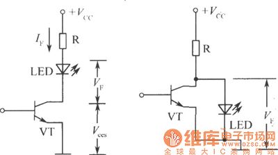
DC LED driver circuit diagram using transistor
Published:2011/6/23 2:51:00 Author:Ecco | Keyword: DC , LED driver , transistor
View full Circuit Diagram | Comments | Reading(2017)
BSR (G) series of LED symbol display appearance circuit diagram
Published:2011/5/17 4:17:00 Author:Ecco | Keyword: BSR (G) series , LED , symbol, display , appearance
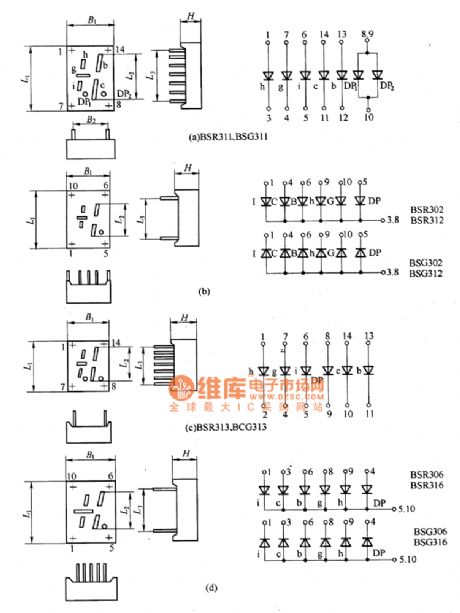
BSR (G) series of LED symbol display
BSR (C) series of LED symbol display uses potassium phosphide light-emitting diodes as light source and reflection cavity cover made by ABC resin to constitute character display. It has the features of small size, low voltage, high brightness, long life and wide view, and it is mainly used in digital displays as the characters.
(View)
View full Circuit Diagram | Comments | Reading(520)
Maintenance circuit diagram of microprocessor partial failure
Published:2011/6/24 2:58:00 Author:Ecco | Keyword: Maintenance circuit , microprocessor, partial failure
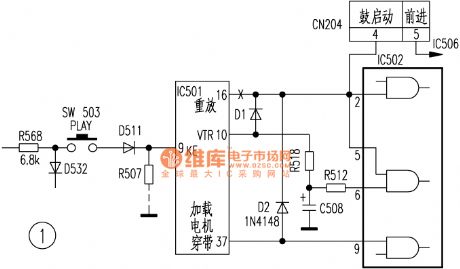
Figure 1 is a schematic diagram of the machine, when you press the playback button PLAY (SW503), pin {18} the address signal of IC501 (μPD7538C) is the high start pulse signal by sent to pin 9 after passing the R568, SW503, D511. The internal circuit of microprocessor will generate IC501 playback control commands, so that pin {16} high will output 4 9V high level, of which one way is sent to the pin 4 of CN204 to drive the drum motor, and another way is sent to pin 2 and pin 5 of IC502. The dominant axis motor of IC501 is positive rolling , the pin {34} of control commands output end is also in high level, which is added to pin 5 of CN204 by IC506 to drive the capstan motor be positive rolling.
(View)
View full Circuit Diagram | Comments | Reading(578)
The circuit diagram composed of ZHF-9901 and ZHJ-9902
Published:2011/5/13 4:28:00 Author:Ecco
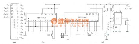
Integrated IR remote control module is a high integrated, fully functional infrared remote control transmitter module. ZHF-9901/03/05 is the transmitting module, ZHJ-9902/04/06 is the receiving module. (b) is a single touch-tone single infrared remote control launcher. (c) is an infrared receiving circuit composed of ZHJ-9902. (View)
View full Circuit Diagram | Comments | Reading(480)
NEC N—831 VCR common breakdown maintenance circuit diagram
Published:2011/6/24 3:50:00 Author:Ecco | Keyword: NEC , VCR, common breakdown , maintenance
When the power switch is turned on, the electronic viewfinder image is normal, pressing the power zoom key T (Telephoto), when the scene is near the target, the inside viewfinder image is blurred. Analysis and Maintenance: When shooting, pressing the T key and when the scene is near the target and the viewfinder image is blurred, it should be noticed that the focus ring does not rotate, then you should check the camera focus selecting switch on the control panel (FOCUS) has been pulled to AUTO position; rotateing the focus ring to observe the clarity of the viewfinder image is back to normal level or not,then you can determine the failure's existence being in auto-focus detection control and motor drive circuit.
(View)
View full Circuit Diagram | Comments | Reading(1121)
| Pages:369/471 At 20361362363364365366367368369370371372373374375376377378379380Under 20 |
Circuit Categories
power supply circuit
Amplifier Circuit
Basic Circuit
LED and Light Circuit
Sensor Circuit
Signal Processing
Electrical Equipment Circuit
Control Circuit
Remote Control Circuit
A/D-D/A Converter Circuit
Audio Circuit
Measuring and Test Circuit
Communication Circuit
Computer-Related Circuit
555 Circuit
Automotive Circuit
Repairing Circuit