
Index 371
MYL21 lightning protection zinc oxide varistor appearance circuit
Published:2011/7/13 10:20:00 Author:Nancy | Keyword: lightning protection , zinc oxide varistor
View full Circuit Diagram | Comments | Reading(418)
zero passage comparison circuit
Published:2011/7/13 10:33:00 Author:Nancy | Keyword: zero passage, comparison circuit
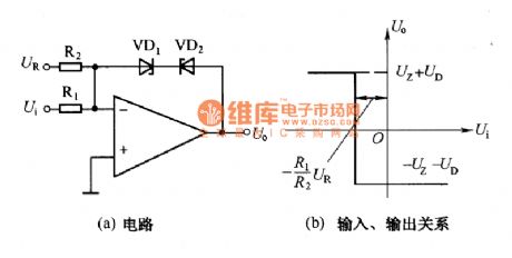
The zero passage comparison circuit, inputand outputrelationshipcurve.
The zero passage comparison circuit is shown as figure (a). In an ideal situation, the relationship between input and output is shown in figure (b), UZ stands for the regulated voltage when the diode works in the reverse voltage and UD stands for the voltage drop when the diode works in the forward voltage. The zero passage comparison circuit is often used in the conversion of signal waveform, such as the sine wave coverting into rectangle wave, etc. (View)
View full Circuit Diagram | Comments | Reading(421)
100kHz 600W power factor correction circuit
Published:2011/7/12 21:36:00 Author:TaoXi | Keyword: 100kHz, 600W, power factor, correction circuit
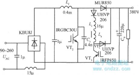
The 100kHz 600W power factor correction circuit (PFC) is as shown in the figure, it uses the ZVT--PWM boost topology. In order to reduce the cost, the main switching tube uses the IGBT tube with the TO-220 appearance which is produced by the IR company; the IRGB30U is connected with the 4.4 nF capacitance, and it has the softening switch function and it reduces the turn-off power loss. Although the auxiliary switch has the low RMS current, but it bears the high turn-off current, so we use the MOSFET tube IRFP450(500V, 16A, 150W).
The circuit output voltage is 380V, the input voltage is AC 90~260V. The efficiency of this power correction circuit has relation ship with the operating range of the input voltage. When the ZVT PFC circuit is operating in the 100kHz, and the AC input voltage is in the range of 180~260V, the total efficiency is 97% ~ 98%.
(View)
View full Circuit Diagram | Comments | Reading(3059)
Double Op-amp Producing Audio Signal Generator Circuit
Published:2011/6/14 13:02:00 Author:Michel | Keyword: Double Op-amp, Producing Audio, Signal Generator Circuit
The sine wave signal generator is often used in test for audio equipment.Hereby,the sine wave signal generator composed of a double op-amp integrated circuit is introduced.This generator has simple circuit,small total harmonic distortion ,supply and the frequency coverage is 76Hz~16kHz.And it uses uses single power supply.
The picture 1 is sine wave signal generator circuit.This circuit is composed of bridge T oscillating circuit,buffer amplifier, neutral voltage generator circuit.The picture's left is oscillating circuit.There is a bridge T circuit between the integrated amp's ① pin and② pin(reversed-phase input terminal) and oscillation frequency is altered via altering bridge T circuit's reference. (View)
View full Circuit Diagram | Comments | Reading(517)
A window comparator circuit made by LTCl042
Published:2011/7/10 2:12:00 Author:leo | Keyword: A window comparator circuit, integrated capacitor
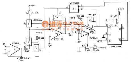
The picture shows a window comparator circuit made by LTCl042. In this circuit, LTC1042 is the window comparator which is used to test integrator and carry out the original reset of it according to the different needs. The first condition of integrator is to select the accuracy of the time periods it needs. After this, the second step is to select the components that can meet the needs of the accuracy, especially the operation amplifier and integrated capacitor. For example, to the operation amplifierμA741 with input differential current of 80 nA, its inaccuracy is 1% when the time period is 0.25 s, however, to LTC1152 with input differential current of 100 pA, its inaccuracy is 1% when the integrated time period is 200 s. In order to improve the accuracy, integrated capacitor uses polystyrene, polytetrafluoroethylene(PTFE) and so on. (View)
View full Circuit Diagram | Comments | Reading(943)
Automatic Transmission Circuit One of Soueast Lioncel
Published:2011/7/8 21:39:00 Author:Michel | Keyword: Soueast Lioncel, Automatic Transmission, Circuit One
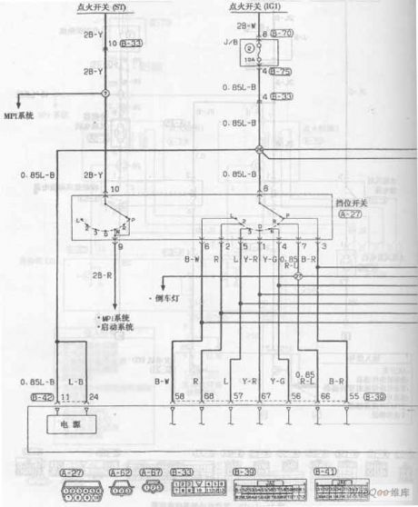
Automatic Transmission Circuit of Soueast Lioncel (View)
View full Circuit Diagram | Comments | Reading(602)
Automatic Transmission Circuit Two of Soueast Lioncel
Published:2011/7/8 21:40:00 Author:Michel | Keyword: Lingshuai Cars, Automatic Transmission, Circuit Three
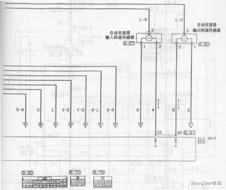
Automatic Transmission Circuit of Soueast Lioncel (View)
View full Circuit Diagram | Comments | Reading(571)
Multichannel Sampling Circuit
Published:2011/6/15 8:46:00 Author:Michel | Keyword: Multichannel, Sampling Circuit
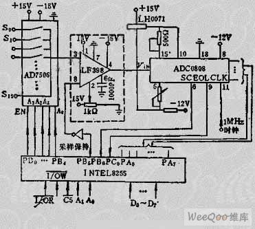
Multichannel Sampling Circuit
The picture is a practical example of multichannel sampling circuit.It consists of 16 channel analog switch, AD7506 type chip, sampling keeping circuit LF398 and AD converter, ADC-0808 and it connects with 1 / O interface chip INTEL8255 parallel port.PA0 ~ PA7 and ADC0808 data is linked together, which is used for data input.PB0 ~ PB4 is channel selection signal which controls the input channel choice.PB5 is the keeping signal, PB6 sampling is the starting signal of A/D converter conversion.PC0 is the end signal input port of A/D converter which is judged by CPU read.Multichannel sampling circuit's work is controlled by corresponding program completely.This circuit has the following kinds of work entirely controlled by the corresponding programs and it has following work ways.
First,sampling in order.It scans sampling aacording to channel sequence.Second,fixed-point sampling.It samples to one fixed channel.Third,setting sampling interval.If the actual measured input signal is less than channel numbers of sampling system , the sampling interval can be narrowed. (View)
View full Circuit Diagram | Comments | Reading(980)
Cadmium Nickel Battery Charging Circuit of Automatic Control and Constant Current Charging
Published:2011/6/15 9:08:00 Author:Michel | Keyword: Automatic Control, Constant CurrentCharging, Cadmium Nickel, Battery Charging Circuit
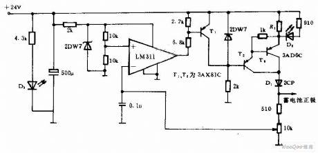

This circuit adopts automatic control,and constant current charging method.The nominal voltage of charged battery is 10V and its end-of-charge voltage is 12V.T2, T3, and related components consistitutes constant current source and the current value is approximate 4.8 V/R1.Diode D1 is set to prevent the battery discharges when AC power goes off or rectifier circuit breaks down.LM311 is comparator outputs low PWL when it reaches setting value fter being charged and T1 saturates and conducts,T2 stops,constant current sources stops working and the charging stops.
LED,D2 brights,D3 is used as source indication when it is charging. (View)
View full Circuit Diagram | Comments | Reading(2001)
Simple Practical Stable and Reliable 5V to 3.3V Circuit
Published:2011/6/15 10:58:00 Author:Michel | Keyword: Simple, Practical, Stable, Reliable, 5V to 3.3V Circuit

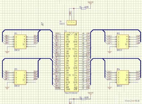
Reducing the power supply voltage can reduce dynamic power consumption thus electronic devices's work voltage drops from 5V to 3.3V even lower value such as 2.5V and 1.8V.Many chips still use 5 V power supply voltage because of kinds of restricting reasons.So in many designs, 5 V logic system and 3.3 V logic system with low voltage coexist.With the introduction of more low voltage standard, different power supply voltage and different logic level device interface problems will exist in a long time, therfore,there is a PWL conversion when devices interface.Level conversion module mainly uses the 74 ALVC164245 devices and it can achieve mutual conversion between 3.3 V voltage and 5 V voltage. (View)
View full Circuit Diagram | Comments | Reading(1405)
General Wireless Alarm Launch and Receiving Circuit
Published:2011/6/15 6:57:00 Author:Michel | Keyword: General Wireless Alarm, Launch, Receiving, Circuit

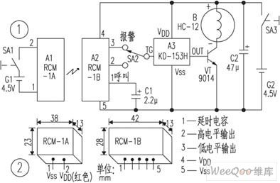
The circuit is showed as the picture and the transmitter is composed of wireless remote control launch module,A1 and battery G1 and the power switch SA1. Receiving alarm consists of wirless remote control receiving module,A2 andsimulated sound integrated circuit A3 etc.
Usually,A1 module built-in antenna launches out into the surrounding space about 250 ~ 300 MHz frequency modulation electromagnetic wave.Within effective distance,the wave is received by tiny receiving antenna inside A2 module.The wave outputs low PWL after its modulatation,amplification,test ,delay and PWL change.A3 does not work because TG PIN's low PWL, acoustic device B has no voice.Once the receiving and launching distance exceeds 15mA2 will be not able to receive enough strong transmitting signal and then A2 low pin changes into high PWL,which tirggers inside circuit work of A3.
(View)
View full Circuit Diagram | Comments | Reading(411)
IC Synchronous Detection Circuit of 2MHZ Input Signal Srequency
Published:2011/6/14 13:06:00 Author:Michel | Keyword: 2MHZ, Input Signal Srequency, IC, Synchronous Detection Circuit
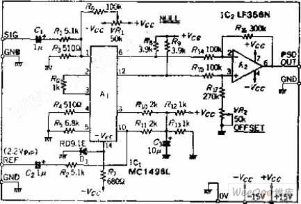
Circuit's Functions
MC1496 is widely used as IC balance modulation circuit, the basic circuit connection are the same with modulation circuit.But it's output circuit adds level shifting circuit so it can be used in synchronous detection and gets EO =E.COSθ output. Without switch circuit, according to the the element parametersof the circuit , the signal frequency reaches 2 MHZ.Circuit's Work PrincipleMC1496 is composed of double transistor differential circuit and its output is open-collector type, and it needs connect outside load resistor.In order to perform the dc coupling and the differential amplifiers receiving A1 output end signal,OP amplifier A2 forms a 3 times constitutes level shifting circuit. (View)
View full Circuit Diagram | Comments | Reading(2321)
Low Frequency FM Circuit of Transistors
Published:2011/7/7 16:18:00 Author:Michel | Keyword: Low Frequency, FM Circuit, Transistors

The picture is low frequency FM circuit of transistors.In this circuit, emitter coupling multivibrator is composed of Vt1 and VT2 and constant current comopsed of VT1 and Vt2 are used between its base and emitter and the base voltage controls the work current.Vt1 and Vt2 can make the VT3's voltage between 0.5~0.6V.If offset voltage is 5 V and the oscillation frequency ≈ 3.3 x1O3 / C1 according to the device parameters and environmental temperature is positive temperature coefficient. VTl is temperature compensation circuit and its purpose diode W knife of base-collector compensates temperature coefficient and at the same time VT1 also can complete level of the shift work of VT4 and VT5 UBE . When the +Ucc-0.6V frequency oscillation signal is taken from the VT3 's collector,it flows through straight capacitance C2 and is added to VT6's base and it outputs frequencysignal from emitter of follower VT6.
(View)
View full Circuit Diagram | Comments | Reading(513)
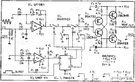
Short Pulse Waveform Generating Circuit of DG201
Published:2011/7/7 15:20:00 Author:Michel | Keyword: Short Pulse, Waveform, Generating Circuit
The picture is a short pulse waveform generating circuit composed of DG201 etc.This circuit is often used for the signal source of measuring sound system transmitting condition or electronic instrument dynamic characteristics.In the circuit,A1's gain is almost 2 and it is used to compensate forthe gain loss of analog switch DG201 and output buffer. When terminal impedance is 600 Ω, circuit's total gain is 1 and it is also used as a buffer meanwhile.
The comparator A2 is used to test positive zero-crossing.It outputs short pulse from sinO° and 74HC74 data latches keeps it synchronous.The output time of the short pulse waveform is provided by outside pulse generator and it is asynchronous with sinusoidal oscillator phase .Thus,on the zero-crossing,74HHC74's Q end outputs high PWL after the short pulse inputing high PWL.It outputs via the buffer composed of VT1~VT4 when the analog switch DG201 conducts. (View)
View full Circuit Diagram | Comments | Reading(392)
Triangle and Square Wave Circuit of LF353
Published:2011/7/7 14:27:00 Author:Michel | Keyword: Triangle, Square, Wave Circuit
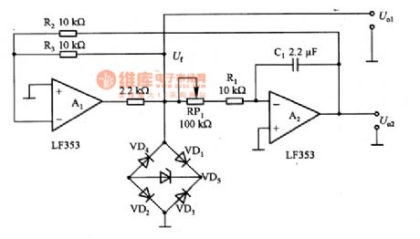
The picture is triangle and square wave circuit composed of LF353.The circuit consists of lag comparator A1 and inverse integrator A2,charging and discharging time constant is determinded by (RRP1 + R1) and C1.Now we explain the the oscillation working principle by positive or negative saturated state of A1 when the power supply turns on.
If A1 outputs positive voltage, limiting circuit composed of VD1~VD5 and its voltage +UoH is equal to the voltage of voltage regulator diode and diode forward voltage.Integrators A2 intergrates + UoH voltage and the output voltage U。2 is equal to -UoH/(RRP1+R1)C1(V/s) and A2 output quickly enters saturated state. (View)
View full Circuit Diagram | Comments | Reading(1654)
Pulse Generator Circuit of CA3130
Published:2011/7/7 14:27:00 Author:Michel | Keyword: Pulse Generator, Circuit

This picture is pulse generator circuit composed of CA3130 etc.This circuit uses VD1 and VD2 diode (2 SK30)with high reverse resistance,which makes the charging and discharging time constant adjusted independently.R1, R2, R3 and A1 constitute comparator and S1 connects different capacity capacitors to obtain different period pulse signal. The high and low PWL timeof output waveformcan be set independently and high PWL time is determined by resistance value setting and low PWL time is decided by RP2 resistance value setting.According to the circuit components parameters, and the output pulse cycle is 4 u 5 ~ 1 S. (View)
View full Circuit Diagram | Comments | Reading(1608)
Stable Frequency and Amplitude Sine Wave Output Circuit
Published:2011/6/14 21:19:00 Author:Michel | Keyword: Stable Frequency and Amplitude, Sine Wave, Output Circuit
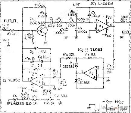
Circuit's Functions The sine wave oscillation circuit requires that oscillation frequency and output level are very steady.It's hard to realize if common CR oscillation circuit is adopted but this circuit can meet the requirement. square wave can be changed into sine wave when low-pass filter is used.But waveform distortion depends on filter's cutoff characteristics and filter's levels should increase and ultraharmonics are greatly reduced to get low distortion waveform.
Circuit's Work PrincipleThe quartzquartz crystal oscillator circuit generating clocksignal frequency is divided into 1KHZ by frequency division circuit.The waveform dutyfactorrate is set to 50%:50% to reduce thedistortion caused by even-order harmonic .It can use binary counting frequency demultiplier directly.
(View)
View full Circuit Diagram | Comments | Reading(733)
Stable Up/Stop Phase Short Pulse Waveform Generating Circuit With Synchronous Circuit
Published:2011/6/14 21:15:00 Author:Michel | Keyword: Synchronous Circuit, Stable Up/Stop Phase, Short Pulse Waveform, Generating Circuit
As function generator,oscillator generates short pulse waveform easily.This circuit has not only normal CR oscillator and pulse generator and also contains additional decoder circuit which produces short pulse generator.Short pulse wave mostly is used as the signal source to test audio equipment transfering status or electronic instrument dynamic characteristics.
Circuit's Work Principle
The OP amplifier A1's magnification time is around 2 times and this is to compensate analog switch or output buffer gain loss , and the general magnification timeis1 and it can be used as buffer.
The comparator A2 begans to output burst wave through SIN0 degree and uses IC4 data-latch to make it become synchronous in order to test signal's zero crossing. (View)
View full Circuit Diagram | Comments | Reading(710)
Ultra-low Frequency Sawtooth Wave Generating Circuit of Common Components
Published:2011/6/14 13:16:00 Author:Michel | Keyword: Common Components, Ultra-low Frequency, Sawtooth Wave, Generating Circuit

Circuit's Functions
People immediately associate with OP amp or miller integral circuit composed of discretes when we mention sawtooth wave. But long cycle ultra-low frequency sawtooth wave generating circuit causes linear deterioration because of OP amp input deviation or integral points capacitor insulation resistance.To solve this problem, we can use counter and D - A converter to make the time cycle not be restricted.But, if the output waveform is amplified it will be trapezoidal.Many D - A converter multiples are required to make the wave looks like it is a linearityand the specific multiples depend on application purposes.
(View)
View full Circuit Diagram | Comments | Reading(981)
Basic Circuit of Thermistance Bridge Type Measuring
Published:2011/6/14 21:56:00 Author:Michel | Keyword: Thermistance, Bridge Type, Measuring, Basic Circuit
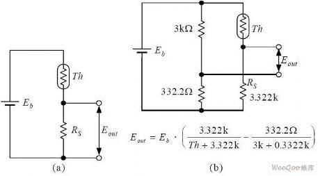
Basic Circuit of Thermistance Bridge Type Measuring (View)
View full Circuit Diagram | Comments | Reading(468)
| Pages:371/471 At 20361362363364365366367368369370371372373374375376377378379380Under 20 |
Circuit Categories
power supply circuit
Amplifier Circuit
Basic Circuit
LED and Light Circuit
Sensor Circuit
Signal Processing
Electrical Equipment Circuit
Control Circuit
Remote Control Circuit
A/D-D/A Converter Circuit
Audio Circuit
Measuring and Test Circuit
Communication Circuit
Computer-Related Circuit
555 Circuit
Automotive Circuit
Repairing Circuit