
Index 373
TL499A switch regulator, main features and pin of DC-DC circuit and power supply monitor
Published:2011/7/10 22:21:00 Author:Lucas | Keyword: switch regulator, main features , pin , DC-DC circuit , power supply monitor
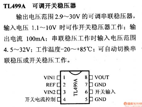
TL499A adjustable switch regulator
It is the adjustable series regulator with output voltage range in 2.9 ~ 30V, when input voltage is 1.1 ~ 10V, it can work as switching regulator; output current is 100mA; the input voltage range is 4.5 ~ 32V when it works as series regulator; Operating Temperature is -20 ~ + 85 ℃; series regulator and switching regulator can be automatically converted.
(View)
View full Circuit Diagram | Comments | Reading(575)
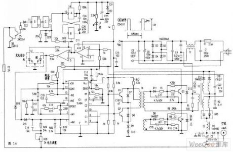
Spinner Weft feelers circuit diagram
Published:2011/6/12 22:59:00 Author:Lucas | Keyword: Spinner , Weft feelers
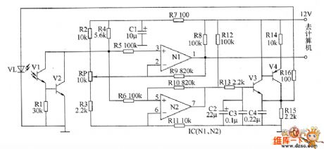
The spinner Weft feelers circuit consists of the optical signal amplifier and LED driver circuit, the circuit is shown as the chart. Optical signal detection amplifier circuit is composed of the infrared phototransistors V1 and V2, resistors R2 ~ R5 and R7 ~ R9, potentiometer RP, capacitor C1 and the N1 which is inside of the operational amplifier integrated circuit IC (N1, N2). LED driver circuit is composed of infrared light-emitting diode VL, transistors V3, V4, resistor sR2 ~ R4, R6, R10 ~ R16, potentiometer RP, capacitors C2 ~ C4 and the op amp N2 which is inside of the IC. R1 ~ R15 select 1/4W metal film resistors; R16 uses 1W metal resistor. RP uses small synthetic carbon potentiometer or variable resistor.
(View)
View full Circuit Diagram | Comments | Reading(785)
Application Circuits of NCP5602 and NCP5612
Published:2011/6/14 12:57:00 Author:Michel | Keyword: Application Circuits
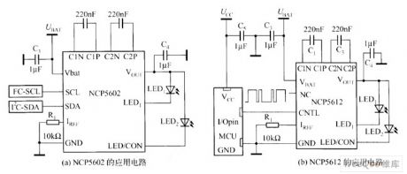
Gradual brightness changes is mainly applied to create the theatre type illuminating effect when portable electronic devices get started or closed.At startup when backlit current will be gradually amplified to 20mA in a predetermined time interval in stepping way and it will be gradually reduced when it gets colsed.Microprocessor sends different frequencies PWM signals to LED drivers' end and the LED current is increased or reduced through many stepping ways in a time interval,which achives the effects.This method shortcoming is that it consumes real-time processor,for example,this happens on NCP5602 and NCP5612's LED driver chips. (View)
View full Circuit Diagram | Comments | Reading(416)
TTL level / ± l2V level conversion circuit
Published:2011/7/6 4:59:00 Author:Lucas | Keyword: TTL level, ± l2V level , conversion circuit
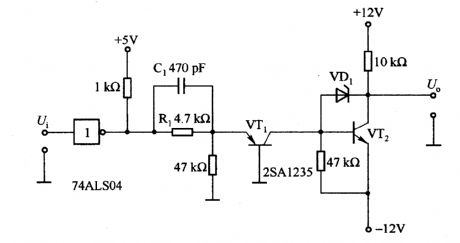
In the circuit, VTl is the switch circuit, of which base is grounded circuit. When 74LSO4 output is in high level, VTl is conducted, and its collector current changes into the base current of VT2, VT1 is also conducted, and the level with the output in U is changed into l2V to add with the collector saturation voltage of VT2. This circuit can not make high-speed switching work. If Rl is connected to capacitor Cl with capacity in several hundred pF in parallel, and the base - collector of VT2 is connected with the Schottky diode VD1, VT2 is conducted and not in the completely saturated state, so to some extent, it will increase the switching frequency.
(View)
View full Circuit Diagram | Comments | Reading(618)
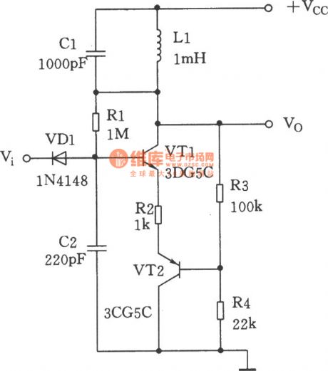
Voltage / frequency conversion circuit composed of NE555
Published:2011/7/10 22:23:00 Author:Lucas | Keyword: Voltage conversion , frequency conversion
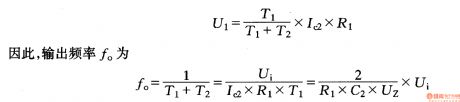
In the circuit, NE555's oscillation frequency is controlled by the VT2, and during its pin 3 in the low output waveform (output waveform of the T1 period), as VTI stops, VT2 is conduction with current Ic2 flowing, and the size is controlled by the output voltage of Al. C2 discharge time T1 = C2U2 / (2Ic2), in the formula, Uz is the stable voltage of VD1. NE555 output is in high level, the current flows VD3 by pin 3. R2 and C2 have current flowing. Then VTl is switched into saturated conduction, and the base of VT2 is equivalent to short-circuit, so VT2 ends, and the collector current Ic2 is zero.
(View)
View full Circuit Diagram | Comments | Reading(4097)
Load Power Adjustor One
Published:2011/6/14 12:50:00 Author:Michel | Keyword: Load Power Adjustor, One
The load power adjustor adopts zero passage adjusting power circuit and the circuit is simple but with good effect.Its dependability is also high and it can regulate kinds of heating appliances' power such as electric hair dryer, electric cooker,electric iron and series wound motor's speed.
Circuit's Work Principle
The bearing power adjustor circuit is composed of power supply circuit,zero passage test circuit and power regulation circuit and it is showed as the picture 5-54.The power supply consists of mains transformer,T,commutation diode,VD1 and VD2 and filter capacitor,C. (View)
View full Circuit Diagram | Comments | Reading(438)
12V,24V battery automatic charger circuit
Published:2011/7/8 3:22:00 Author:Fiona | Keyword: 12V,24V battery automatic charger
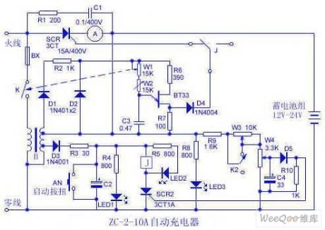
unijunction transistor BT33, C3, W1, W2 and other components form the relaxation oscillator.The pulse signal produced by he relaxation oscillator is transmited through isolation diode D4 to the control pole of thyristor SCR1 , adjusts the resistance of W1 to change the trigger the conduction angles of SCR1, which changed the charge current. Thyristor SCR2, relay J, W3, W4, D5 and other components form the storage battery in automatic protection circuit, when the battery voltage isfillingto the upper limit the W3, W4 set, D5 breakovers, SCR2 is triggered to breakover, LED2 display and relay picks, at the same time J switches to the normally open, cuts off SCR1 control pulses focused, that is to stop charging the battery. K2 is 12V, 24V battery charging switch, the icon places12V stalls.
(View)
View full Circuit Diagram | Comments | Reading(4311)
Typical half bridge type electric bicycle battery charger circuit
Published:2011/7/8 3:22:00 Author:Fiona | Keyword: Typical half bridge type, electric bicycle battery charger
Discharge switch is a breakover of transistor Q6, Q6, its collector and emitter make the storage battery short out, storage battery discharges. Q6 is off, the storage battery restores charge.Q5 and Q6 aredirect coupling, commonly known as Darlington. Q6 is controlled by loading negative pulses and the oscillator. Loading negative pulse control is formed by the C and D of the IC3. D is connected as inverter ,only when the both inputs of C are high level, ③ pin is low level, it is opposite through the D to make the Q6 breakover to discharge for the storage battery.The ② feet of C comes from per second 1 (pulse width 3ms) positive pulse of the multivibrator ,the ① feet of C comes from the ① feet of two-phase current detection circuit IC2.When constant current is charging, ① pin is high level. At this point, the negative pulse is applied.
(View)
View full Circuit Diagram | Comments | Reading(4161)
practical lithium battery quick charger circuit
Published:2011/7/8 3:22:00 Author:Fiona | Keyword: practical lithium battery, quick charger
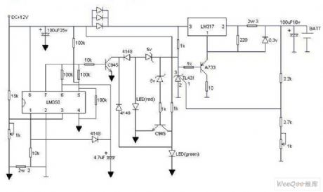
The circuit has a function of displaying the charging status.It is charging when the red light flashes and it will be full when the green light flashes, the green light means it is fully charged. As long as you have a 12V power supply, then do not replace the battery after completing the circuit, adjust the adjustable resistance at the lower right corner to make the battery output is 4.2V, and then adjust the adjustable resistance at the lower left corner to make the third pin of LM358 is 0.16V,and the charge current is 380mA, ultra-fast, three parallel diodes are used to step down and to prevent overheating LM317,and LM317 should add the heat sink, the transistor of the figure can be any type. (View)
View full Circuit Diagram | Comments | Reading(656)
Good balance,wide selection of current balance constant current output circuit
Published:2011/7/8 3:21:00 Author:Fiona | Keyword: balance constant current output
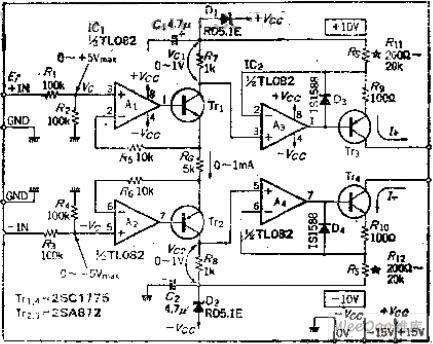
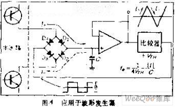
Circuit Work
OP amplifiers A1 and A2 are to change the unipolar input circuit to a differential input circuit that the balance is good and change the 0 ~ 10V input to 0 ~ 1MA output (B = 10V, divided by R1, R2 , current is determined by the RO, RO = 5K, it is the resistance of the selected magnification), if R7 = R2, then the voltage generated at both ends of R7, R2 will be equal, namely:
If it is required to generate asymmetric waveform, as long as the R7 is not equal to R2, VC1 and VC2 can not be equal. It can also be used to generate the sawtooth.
OP mplifiers A3, A4 is a symmetrical circuit, respectively use +10 V and-10V as the base power, you can get I + = VC1/R11, I-= VC6/R12 constant current,change resistors R11 and R12's resistance or change V0 to do the current range switching.If R11 changes at 200Ω~2000Ωfor the unit with 10 times, VC1 = 1V, the circuit can get the constant current output that I + = 5MA, 500UA.
Figure A is the block diagram of unction generator waveform form part, the capacitor C is to constant current charge and discharge, it can produce a good linear triangular wave.
(View)
View full Circuit Diagram | Comments | Reading(761)
Humidity measurement circuit with temperature compensation
Published:2011/7/1 5:47:00 Author:Fiona | Keyword: Humidity measurement, temperature compensation
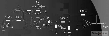
In the actual application,it needs to consider linear processing and temperature compensationfor humidity sensor,and often uses operation amplifier to constitute humidity measurement circuit.The figure is the humidity measurement circuit.Rt is thermosensitive resistor (20kΩ, B = 4100K); RH is the H204C humidity sensor,operational amplifier type is LM2904.Humidity voltage characteristics and temperature characteristic of the circuit demonstrate that: in (30% ~ 90%) RH, 15 ℃ ~ 35 ℃ range,the humidity errorexpressed bythe output voltage is less than 3% RH. (View)
View full Circuit Diagram | Comments | Reading(1250)
Electric firebug circuit
Published:2011/7/10 23:41:00 Author:leo | Keyword: firebug circuit
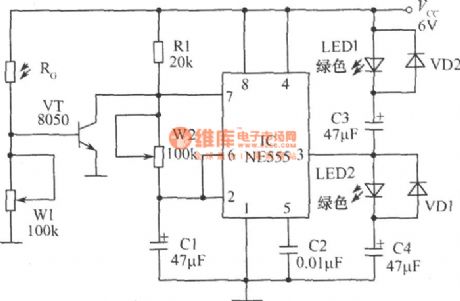
As it is known to all, the brightness of firebug can only be seen clearly at night, which is because its brightness is not the same as that of the twinkling color lamps. The brightness of the color lamps is monotonic but that of the firebug is changing from strong to weak and its short-lived and super bright. This circuit is designed based on the emitting principle of firebug. NE555, R1, W2, C1, C2 form the multivibrator while RG, W1 and VT form light activated circuit. Mimic bus is made up of LED1, LED2, VD1, VD2, C3 and C4. (View)
View full Circuit Diagram | Comments | Reading(672)
Shared RF and base oscillator
Published:2011/7/10 23:16:00 Author:leo | Keyword: Shared RF, shared base
The picture shows a simple oscillator with high stability. It can start automatically with the work voltage of 12 V and work current of 1mA. Its drive circuit is D type amplifier with low output resistance and high output amplitude. Its work voltage coverage is from 2 V to 24 V and it also has other excellent features. Oscillator frequency is decided by LI and CI. As the picture shows, when the frequency of the selected component is 160kHz, time constant RI and CI will be longer than oscillating period. (View)
View full Circuit Diagram | Comments | Reading(829)
TA8164P-AM/FM former stage radio integrated circuit
Published:2011/7/5 8:44:00 Author:chopper | Keyword: AM/FM, former stage, radio, integrated circuit
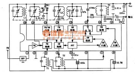
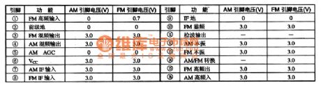
TA8164P is a former stage radio integrated circuit,and it is applied to radio system like low-voltage radio,tape recorder .1.The inner circuit and function of pins of TA8164PTA8164P integrated package includes AM high level circuit, local oscillator circuit, mixing circuit,medium level circuit and detector circuit;FM high-level, local oscillator, mixing, medium level,frequency discriminating circuit; and ACC circuit, FM / AM band selection circuit. The inner circuit and typical application circuit of integrated circuit are shown as picture 1.
(View)
View full Circuit Diagram | Comments | Reading(4467)
Swedish Leica card laser rangefinder
Published:2011/7/6 7:09:00 Author:chopper | Keyword: swedish, Leica card, laser rangefinder

View full Circuit Diagram | Comments | Reading(371)
South Korea Imported Anti-static PVC Board of Shuangzhen Supply
Published:2011/6/25 4:31:00 Author:Michel | Keyword: Shuangzhen Supply, South Korea, Imported, Anti-static, PVC Board

Shuangzhen supplies South Korea imported anti-static PVC board.Shenzhen Shuangzhen Electronic Co., Ltd is found in Feb. 2007 which has office and warehouses. We are specialied in providing anti-static organic glasses.We devote to providing high-quality industrial products to meet the special needs of high-tech times industry and provide good after-sales service.
Shenzhen/Suzhou/Shanghai/Dalian has South Korea imported anti-static PVC board in stocks.The surface resistance is10^6~10^8Ω with excellent antistatic properties.The appearance isbeautiful and the surface is very smooth.Antistatic properties are not easily affected by temperature and humidity. (View)
View full Circuit Diagram | Comments | Reading(572)
Deep Discussion: Clamp Type Current Transformer Circuit
Published:2011/7/1 18:47:00 Author:Michel | Keyword: Deep Discussion, Clamp Type, Current Transformer, Circuit
SP series clamp type current transformer belongs to precision current transformer category and it is a high precision AC current converter,for example,Praise verification tester for electric power, multi-function watt-hour meter, power analyzer, oscilloscope, digital multimeter , cable faults, double clamp detector type earthing resistance tester, double clamp type phase volt-ampere table, etc.In the constant state of being measured open road, kinds of electric parameters are measured and compared.
The series products production and manufacturing strictly abide by GB1208-1997 Current Transformer and JJG31-1994 Measuring Current Transformer Verification Regulation. (View)
View full Circuit Diagram | Comments | Reading(507)
Single-end Flyback DC-DC Converter Circuit
Published:2011/6/24 0:54:00 Author:Michel | Keyword: Single-end, Flyback, DC-DC, Converter Circuit
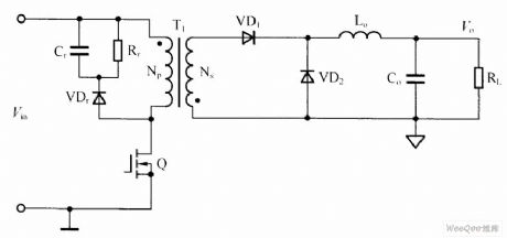
The single-end flyback DC-DC converter circuit is shown as above.Among them,transformer acts as isolation,transmission,energy storage.That's to say,Np stores energy when switch tube Q turns on and Np release energy to Ns when switch tube Q shuts off.A low-pass filter composed of a inductor Lo and capacitance Co is added to the output side,transformer primary level Cr, Rr and VDr constitute RCD leakage peak absorbing circuit.In output loop,a VD1 rectifier diode is needed.If the transformer uses the magnetic core with wind gap,the copper loss is big and temperature rising is relatively higher and its output ripple voltage is larger.But its advantage is that the circuit structure is simple and is suitable for less than 200W power supply. (View)
View full Circuit Diagram | Comments | Reading(807)
Double-tube Forward DC-DC Converter Circuit
Published:2011/6/24 1:15:00 Author:Michel | Keyword: Double-tube, Forward, DC-DC, Converter Circuit
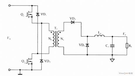
Double-tube forward DC-DC converter circuit is shown as above.Among them,transformer T1 acts as isolation and transformation and and inductance Lo(flow current inductance) is added to output port which acts as energy storage and transmission.The transfomer primary level does not need reset winding because both VD1 and VD2 conduction limit the voltage which two regulation tubes bear when they are turned off.In output loop ,a rectifier diode VD3 and a free-wheeling diode VD4 (VD3, VD4 had better choose the rectifier diode with short recovery time )are needed.Output filter capacitance Co should chooselarge capacity capacitance with low equivalent resistance to reduce the ripple voltage(other topology structure also require like this).
Picture:Double-tube Forward DC-DC Converter Circuit (View)
View full Circuit Diagram | Comments | Reading(815)
Half Bridge DC/DC Converter Circuit
Published:2011/6/24 1:36:00 Author:Michel | Keyword: Half Bridge, DC/DC, Converter Circuit
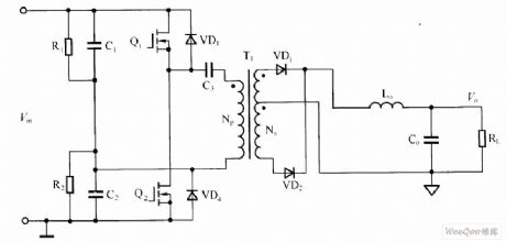
The half bridge DC/DC converter circuit is shown as above.Among them,transformer acts as isolation and transfering energy. Np winding bears half input voltage and vice edge winding voltage make VD1 conducts when switch tube Q1 conducts and vice versa.In the output, VD1, VD2 Lo and Co constitutes rectifier filter circuit. (View)
View full Circuit Diagram | Comments | Reading(5004)
| Pages:373/471 At 20361362363364365366367368369370371372373374375376377378379380Under 20 |
Circuit Categories
power supply circuit
Amplifier Circuit
Basic Circuit
LED and Light Circuit
Sensor Circuit
Signal Processing
Electrical Equipment Circuit
Control Circuit
Remote Control Circuit
A/D-D/A Converter Circuit
Audio Circuit
Measuring and Test Circuit
Communication Circuit
Computer-Related Circuit
555 Circuit
Automotive Circuit
Repairing Circuit