
Index 380
the sawtooth-wave circuit of complementary tube
Published:2011/6/30 6:11:00 Author:Fiona | Keyword: sawtooth-wave, complementary tube
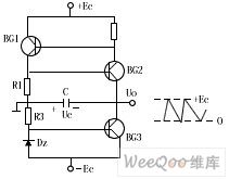
The picture shows the sawtooth-wave circuit of complementary tube.This is self-oscillating complementary sawtooth-wave circuit which the switching device is composed of BG1,BG2 and controls the timing capacitor C to charge and discharge,BG3 is constant flow pipe.When BG1, BG2 are closed, the constant current Ic3 charges to C(polarity is shown as the picture) the output voltage uo decreases with linear time, this is a scanning voltage positive process, when the capacitor voltage Uc drops to the BG2 conduction valve voltage, BG2 starts to conduct,BG1,BG2 arrive at the saturated state after a positive feedback chain reaction,at this time, when you reach a saturation point C remains at saturation without returning to the OFF state through BG1, BG2.
(View)
View full Circuit Diagram | Comments | Reading(592)
complementary tube monostable circuit
Published:2011/6/30 6:35:00 Author:Fiona | Keyword: complementary tube, monostable
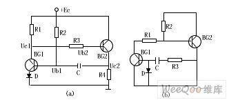
Picture shows the two forms of complementary tube monostable circuit, Figure (b) is complementary tube monostable circuit which the two tubes keep saturation in ordinary state. When it meets conditions,R2 <β1,R1 and R3 <β2, R4,the circuit is in two tubes steady states,when the negative pulse is used at the base BG1, BG1 is out of saturation, and causes a reaction Uc1 ↑ → Ub2 ↑ → Uc2 ↓ → Ub1 ↓.The result of a positive feedback chain reaction is that BG1, BG2 are closed, this is the temporary steady state.At this point C discharges to power supply through R2, R4,it enters two tube saturated stable state after discharging.Diode D is to prevent voltage of C puncturing BG1's base - emitter junction, the pulse width is:
tr=0.7(R2+R4)C
(View)
View full Circuit Diagram | Comments | Reading(901)
Block Circuit Diagram of Internal LM567CN Integrated Circuit
Published:2011/6/15 8:20:00 Author:Vicky | Keyword: Block Circuit Diagram
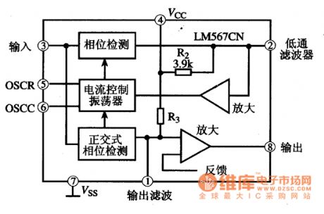
LM567CN is a PLL audio coding integrated circuit. A high-powered cordless phone often uses two pieces of this circuit, taking charge of identifying pilot frequency signal when mobile is off hook and calling signal of the mobile to host machine respectively. (View)
View full Circuit Diagram | Comments | Reading(987)
Typical Applied Circuit Diagram of LM567CN Integrated Circuit
Published:2011/6/15 8:19:00 Author:Vicky | Keyword: Typical Applied Circuit Diagram
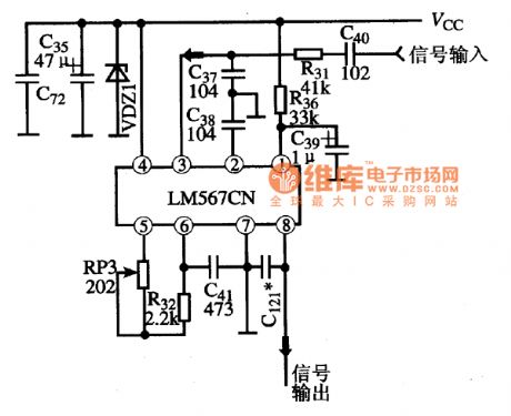
Typical Applied Circuit
Typical applied circuit of decoding circuit, which is composed of LM567CN Integrated Circuit, is shown in the following picture.
(View)
View full Circuit Diagram | Comments | Reading(3119)
Typical Appied Circuit Diagram of LM1036N Integrated Circuit
Published:2011/6/15 8:15:00 Author:Vicky | Keyword: Typical Applied Circuit Diagram
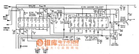
Picture: Typical Applied Circuit of LM1036N Integrated Circuit
Typical Applied Circuit
Typical Appied Circuit Diagram of LM1036N Integrated Circuit is as shown in the picture. (View)
View full Circuit Diagram | Comments | Reading(1949)
Internal Circuit Block Circuit Diagram of LM1203 Integrated Circuit
Published:2011/6/15 8:15:00 Author:Vicky | Keyword: Internal Circuit Block Circuit Diagram
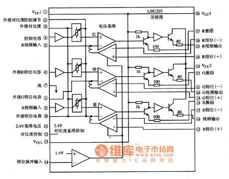
Picture:Internal CircuitBlock Circuit Diagram of LM1203 Integrated Circuit
Functions and Characteristics
The interior of LM1203 integrated circuit is made of three circuits of the same functions, including video small-signal processing circuit, contrast basic control circuit and clamp pulse, and some other adjunct circuits. The internal circuit block diagram is as shown in the picture. (View)
View full Circuit Diagram | Comments | Reading(1131)
Typical Applied Circuit Diagram of LM4610 Integrated Circuit
Published:2011/6/15 8:09:00 Author:Vicky | Keyword: Typical Applied Circuit Diagram
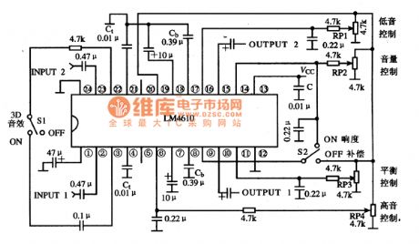
Typical Applied Circuit
Typical applied circuit diagram of LM4610 integrated circuit is shown in the following picture. The LM4610 circuit uses 4 potentiometers MU-M as bass control, volume control, treble control and balance control respectively.
Hint: Left/Right acoustical signal enter LM4610 from (2) pin and (23) pin, get out from (10) pin and (15) pin after processed by the sound volume, tone, balance and 3D audio, and then go to the post-stage circuit. It can be justified that whether LM4610 works regularly by this four pins.
(View)
View full Circuit Diagram | Comments | Reading(2899)
Typical Applied Circuit Diagram of LM8363D/DH Integrated Circuit
Published:2011/6/15 8:07:00 Author:Vicky | Keyword: Typical Applied Circuit Diagram of LM8363D/DH Integrated Circuit,
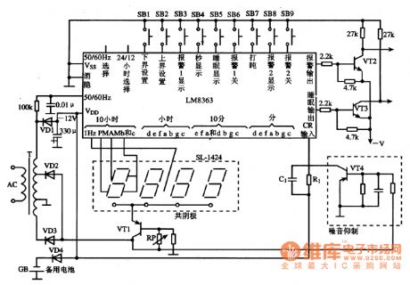
Picture: Typical Applied Circuit of LM8363D/DH integrated circuit
Typical applied circuitTypical applied circuit diagram of digital circuit ,which is composed of LM8363D/DH integrated circuit, is as shownin the picture.
Hint: LM8363 integrated circuit can be thereserve when the power is cut off, and selection method of the value reuired by the osillator is listed below:
grade of 60Hz:R1=130k、C1=0.0068μF,f。=1.92kHz;
grade of 50Hz:R1=150k、C1=0·0068μF,f。=1.6kHz. (View)
View full Circuit Diagram | Comments | Reading(2247)
Hall proximity switch CNC machine tool PLC circuit
Published:2011/7/5 22:02:00 Author:Christina | Keyword: Hall proximity switch, CNC machine tool, PLC circuit
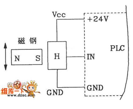
This circuit can be used in the CNC machine tool programmable controller, the precision can be 0.02mm, also it can be used in the high speed punches, the material cutting and feeding of the complex molds, and the stroke control.
(View)
View full Circuit Diagram | Comments | Reading(916)
Two-wire type smart Hall sensor IC application circuit
Published:2011/7/6 1:38:00 Author:Christina | Keyword: Two-wire type, smart, Hall sensor, IC, application circuit
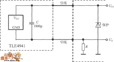
The typical application circuit of the TLE4941 is as shown in the figure. We can change the input current into the voltage signal Vo by using the resistance R, and this voltage signal is connected with the digital voltmeter (DVM) or sent to the single-chip microcomputer with the ADC.
(View)
View full Circuit Diagram | Comments | Reading(591)
The typical application of AD8318
Published:2011/7/6 2:54:00 Author:Christina | Keyword: typical application
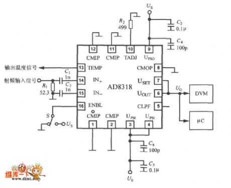
The typical application of AD8318 is as shown in the figure. The AD8318 is designed to measure the 8GHz RF power, so the insulativity of the IN+, IN- pins and functional unit circuits is very important. The positive power supply port UPSI and UPSO must be connected to the same voltage, the UPSI port supplies the bias voltage to the input circuit, the UPSO port supplies the bias voltage to the low-noise output driver of the UOUT port. There are some independent public places in the AD8318. The CMOP can be used as the public place of the output driver. All the public places need to connect with the low impedance PCB ground area.
(View)
View full Circuit Diagram | Comments | Reading(747)
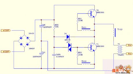
Electronic ballast principle circuit
Published:2011/7/6 2:55:00 Author:Christina | Keyword: Electronic ballast, principle circuit
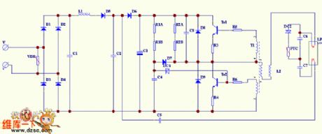
Figure: The Electronic ballast principle circuit
(View)
View full Circuit Diagram | Comments | Reading(1383)
The typical application of LTC5507
Published:2011/7/6 3:11:00 Author:Christina | Keyword: typical application
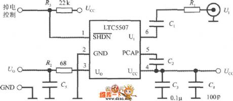
The typical application of LTC5507 is as shown in the figure. C1 is the coupling capacitance of the RF input port, C2 is the peak keeping capacitance, both of C1 and C2 use the ceramic capacitor, the capacitive reactance is lower than 5Ω to reduce the ripple wave of C2. The capacities of C1 and C2 depend on the minimum input frequency fmin of the RF (the unit is MHz), the formula is C1=C21≥(30fmin). In this formula, the units of C1 and C2 are μF. Because the value of C2 will affect the conversion rate and the bandwidth, so C1=C2. The capacities of C1 and C2 can not be too large, or the frequency will exceed the minimum input RF frequency.
(View)
View full Circuit Diagram | Comments | Reading(942)
Digital output angle sensor signal conditioner application circuit diagram
Published:2011/7/1 1:55:00 Author:Ecco | Keyword: Digital output , angle sensor , signal conditioner , application
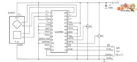
the chart shows the UZZ9001 typical application circuit. C is the decoupling capacitor. SPI input / output interface is directly matched with a microcontroller (μC), which can be set by SCM UZZ9001. UZZ9001 angle measurement error is about ± 0.35o.
(View)
View full Circuit Diagram | Comments | Reading(739)
The application circuit diagram of 1B32 multiple pressure sensor
Published:2011/6/30 2:53:00 Author:Ecco | Keyword: application, multiple , pressure sensor
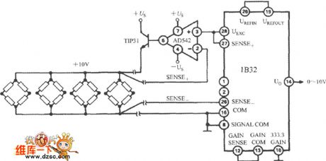
Excitation power can drive multiple bridge sensors after passing AD542, TIP32. AD542 is an op amp which uses Bi-FET as the input stage, and it play the role of starting buffer. TIP31 is the extension NPN power transistor with the maximum reverse voltage in 45V, the maximum collector current in 3A, maximum power consumption in 40W. The circuit can provide +10 V, 300mA excitation source in the temperature range of -25 ~ +80 ℃. When 333.3 GAIN of 1B32 is grounded, the gain is set to 333.3 times.
(View)
View full Circuit Diagram | Comments | Reading(896)
Using capacitor to reduce the cut-off frequency circuit diagram
Published:2011/6/30 22:51:00 Author:Ecco | Keyword: capacitor, reduce , cut-off frequency
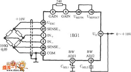
The cut-off frequency of low-pass filter can be set under 1kHz by the external capacitors CSEL1, CSEL2 to meet the needs of narrow-band applications, and the circuit is shown as the chart.
(View)
View full Circuit Diagram | Comments | Reading(539)
Simple touch delay switch circuit diagram
Published:2011/6/27 4:41:00 Author:Ecco | Keyword: Simple , touch , delay switch
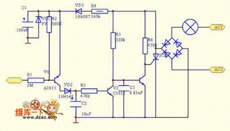
Many people live in high-rise housing have installed sound delay switch in front of their doors, they are easy to use, you can also save energy, but sometimes it did not convenient. This voice-activated switch is very sensitive that the slightest sound will cause it action, such as the sound of neighbors opening and closing door, firecrackers outside, and they will make your door lights be lit up, and it does not save power, but also affect the life of the lam. The circuit is very simple, when touching metal films, VT1 is turned on and charging for capacitor C2.
(View)
View full Circuit Diagram | Comments | Reading(993)
Small (2-3 meters) neon electronic transformer circuit diagram
Published:2011/7/1 1:42:00 Author:Ecco | Keyword: 2-3 meters, neon , electronic transformer
View full Circuit Diagram | Comments | Reading(4005)
The typical application circuit of the LT5504
Published:2011/7/6 20:35:00 Author:Christina | Keyword: typical application
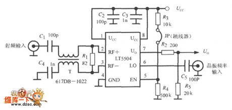
The typical application circuit of the LT5504 is as shown in the figure. The RF signal adds to the RF input port of LT5504 through the coupling capacitance (C1) and the 1:1 RF input transformer (T). R1 is the shunt resistor. The crystal frequency adds to the LO port through the C5. The Uo port gets the DC output voltage Vo through the voltage divider R2 and R5. JP is the jumper, because the R4>>R3, so when the JP is connection, the EN port connected with the high level to open the circuit, when the JP cuts off, the EN port connected with the low level to close the circuit, the chip is in the low power consumption mode.
(View)
View full Circuit Diagram | Comments | Reading(565)
Touching delay lamp switch circuit(9)
Published:2011/7/1 2:37:00 Author:Ecco | Keyword: Touching , delay lamp , switch
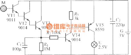
The chart shows the touching delay lamp for night, if you wake up at night and want to know the time, as long as to touch the small box beside the pillow, small light in box E will be lit and turned off after delaying more than ten seconds.
(View)
View full Circuit Diagram | Comments | Reading(501)
| Pages:380/471 At 20361362363364365366367368369370371372373374375376377378379380Under 20 |
Circuit Categories
power supply circuit
Amplifier Circuit
Basic Circuit
LED and Light Circuit
Sensor Circuit
Signal Processing
Electrical Equipment Circuit
Control Circuit
Remote Control Circuit
A/D-D/A Converter Circuit
Audio Circuit
Measuring and Test Circuit
Communication Circuit
Computer-Related Circuit
555 Circuit
Automotive Circuit
Repairing Circuit