
Index 381
Two-dimensional lantern controller circuit analysis and manufacture
Published:2011/6/30 2:59:00 Author:Ecco | Keyword: Two-dimensional , lantern controller , analysis , manufacture
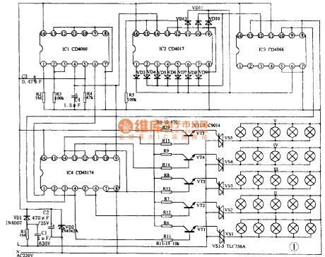
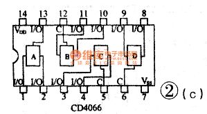
Two-dimensional lantern controller circuit shown in Figure 1 is mainly composed of the NOT gate lCl (CD4069), counting, timing distribution circuit IC2 (CD4017), analog electronic switch IC3 (CD4066) and D trigger IC4 (CD40174). CD4069 logic function and pin is shown in Figure 2a, of which NOT gates F1, F2 and external resistors R2, R3, capacitor C4 form multivibrator to produce a square wave pulse in about 3Hz. R3, C4 are the oscillator timing components. Regulation the two components can change the oscillation frequency.
(View)
View full Circuit Diagram | Comments | Reading(938)
5 v turning to 3.3 v level conversion circuit diagram
Published:2011/6/30 3:11:00 Author:Ecco | Keyword: 5 v , turning , 3.3 v , level conversion
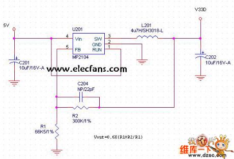
The picture shows the MP2104 circuit produced by the MPSwhich can used inPIN-PIN and RT8008 chip, etc.
(View)
View full Circuit Diagram | Comments | Reading(432)
Discrete sound and light control stairs delay switch circuit(9)
Published:2011/6/30 1:09:00 Author:Ecco | Keyword: Discrete , sound , light , control, stairs delay switch
The unique sound and light control stairs delay switch circuit shown in the Figure has higher sound control sensitivity. at night, when someone walking on the stairs, the footsteps will make electronic switch, lamp light, and after people left, the lights will go off after 30s.
(View)
View full Circuit Diagram | Comments | Reading(925)
Discrete sound and light control stairs delay switch circuit(6)
Published:2011/6/30 1:47:00 Author:Ecco | Keyword: Discrete, sound , light , control , stairs delay switch
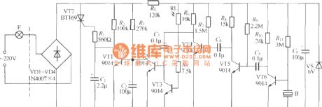
The sound and light control stairs delay switch circuit shown as the chart uses an improved piezoelectric ceramics for the sound -power transducer, due to the sensitivity to sound signal of piezoelectric ceramics is lower than electret condenser microphone, the audio amplifier uses VT4 ~ VT6 three voltage amplification to enhance the switch's responsiveness to sound. Circuit delay time is mainly decided by R3, C2, and the icon data is about 1min.
(View)
View full Circuit Diagram | Comments | Reading(761)
Efficient white LED driver circuit
Published:2011/6/28 2:18:00 Author:Ecco | Keyword: Efficient, white LED , driver circuit
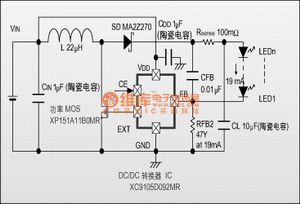
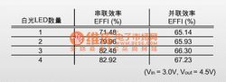
1. The white LED can be used in seies, regardless of the number of connection of the LED, a resistor can provide them with a constant current; 2. A LED resistor can adjust the operating current of white LED; 3. Ceramic capacitors can be used to obtain low ripple noise, and extend the life of the circuit; 4.It can greatly reduce circuit space: XC9105 and FET + SD are available in SOT23 packages, nad the maximum coil thickness is only 1.2 mm, the input and output capacitors are ceramic capacitors.
(View)
View full Circuit Diagram | Comments | Reading(870)
The golf AUM motor circuit
Published:2011/7/4 4:25:00 Author:Seven | Keyword: golf, AUM motor
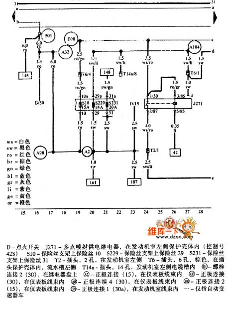
The golf AUM motor circuit is shown as above.
D-lighting switch; J271-multiple injection power supply relay, which is in the protecion shell on the left side of the engine room(the control No. is 428);S10-fuse on the holder 10; S229-fuse on the holder 29; S231-fuse on the holder 31; T2-plug, 2 holes, on the left side of the engine room; T6-plug,6 holes,brown, in the plug protection shell, on the left side of the flow tank; T14a-plug, 14 holes, on the left side of the wire way in the engine room (View)
View full Circuit Diagram | Comments | Reading(1053)
The gate drive circuit with the maximum 90% duty cycle
Published:2011/7/4 22:46:00 Author:Lucas | Keyword: gate drive , maximum , 90%, duty cycle
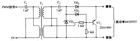
The key of the circuit is that the capacitive coupling circuit and VD1 form the clamp circuit. The output signal of secondary side in pulse transformer Tl is positive, that means up is positive while under is negative, the output signal can make VD2 and VD3 turn off by C2 to provide drive signal for the power MOSFET gate and make it turn on; Tl secondary side output signal is negative, that means up is negative while under is positive, due to the clamping effect of VD1, VD2 and VD3 are turned off, VTl is saturated conduction, the power MOS-FET gate charges and discharges rapidly to reduce the power MOSFET on / off delay time.
(View)
View full Circuit Diagram | Comments | Reading(788)
The interface circuit between MOSFET and logic level composed of NE555
Published:2011/7/4 22:32:00 Author:Lucas | Keyword: interface circuit , MOSFET , logic level
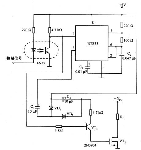
In the circuit, NE555 is the astable multivibrator with the oscillation frequency in 70KHz, and it uses the control input signal of reset pin (pin 4) to control its oscillation on / off state. When pin 4 input is in high level, the oscillator generates oscillation, and low level will stop the oscillation. The pin 3 of NE555 output can provide input voltage for the doubler rectifier circuit composed of VD1, VD2, C3 and C4 form provides the input voltage doubler rectifier circuit, then the output of the doubler rectifier circuit is about 8.5 V. Control signal can control VT2 on-off state, and the load of VT2 can be a relay.
(View)
View full Circuit Diagram | Comments | Reading(2507)
The DC motor servo circuit with compensation performance composed of μA709
Published:2011/7/2 20:50:00 Author:Lucas | Keyword: DC motor , servo circuit , compensation performance
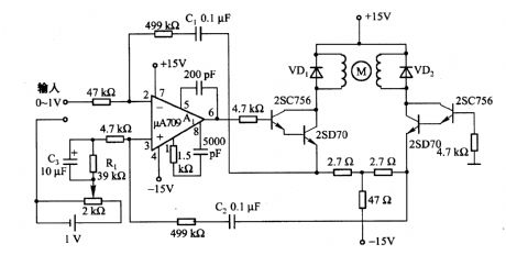
The circuit is used for small self-balancing recorder. The input stage uses the μA709 high-gain op amp, and output power amplifier stage uses differential amplifier. The circuit is added the feedback to reach the desired frequency characteristics.Integral feature is achieved by connecting Cl, C2 in series in the feedback circuit and differential compensation, and the time constant is determined by C3 and Rl. If Cl, C2 are shorted, the error of the system converted to the input is about lOmV. Afetr connecting Cl, C2 and accessing integral compensation, and the loop gain is about more than 7,000 times, so the static error is zero.
(View)
View full Circuit Diagram | Comments | Reading(2616)
DC motor servo circuit composed of μA741
Published:2011/7/4 19:10:00 Author:Lucas | Keyword: DC motor, servo circuit
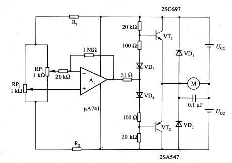
In the circuit, R1 and R2 is to limit all power supply voltage to add on the bridge, and thus change the size of the input signal. RP1 is used for the location set, but the servo motor position is mainly depends on the another voltage signal. At this time, if Al's inverting input end is applied voltage signal, the servo finally steady state is to make the potential of RP2 and the input signal of inverting input end be the same. The bases of VTl and VT2 power transistors are connected with diodes VD3 and VD4 to skillfully applied bias.
(View)
View full Circuit Diagram | Comments | Reading(4596)
33MHz multi-output clock driver circuit
Published:2011/7/5 6:06:00 Author:Lucas | Keyword: 33MHz , multi-output , clock, driver circuit

It is the clock driver circuit composed of P149FC32805, and the maximum clock frequency is 133MHz. It is suitable for the distribution of clock signal in the substrate. Each output delays in less than 270ps and is easy to do synchronization management.
(View)
View full Circuit Diagram | Comments | Reading(571)
The drive circuit of bridge sensor
Published:2011/7/4 22:50:00 Author:Lucas | Keyword: drive circuit , bridge sensor
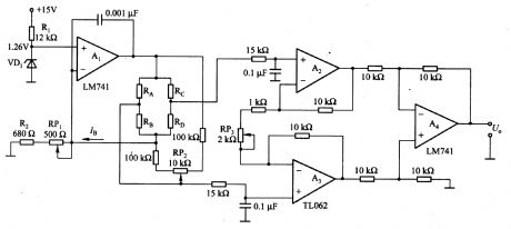
In the circuit, Al is the constant current output circuit, and constant value is decided by the UZ (VD1 stable voltage) and (R (RP1) + R2), and it is bridge sensor (RA-RD constitute a bridge circuit) to provide constant current bias. A2-A4 constitute an instrumentation amplifier, which can amplify the small signal output by sensor to the needed level.
(View)
View full Circuit Diagram | Comments | Reading(583)
The thyristor trigger circuit composed of photocoupler
Published:2011/7/5 3:57:00 Author:Lucas | Keyword: thyristor , trigger circuit , photocoupler
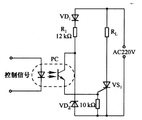
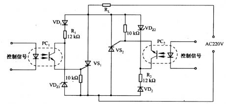
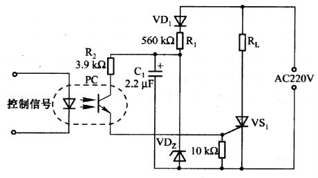
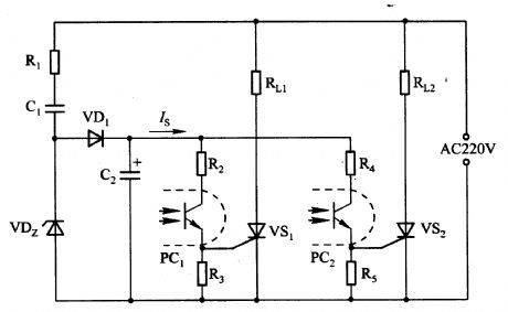
2-5 (a) is a half-wave circuit. Power supply can provide trigger current for the VSl by resistor R1 and transistor in the PC. The circuit is designed to limit Rl power to be as small as possible, and the current conduction angle controlling range shoule be as large as possible. VDl makes the power consumption of Rl halve, VD2 is used to limit the PC collector transistor cut-off voltage. Figure 2-5 (b) is a full-wave power. Figure 2-5 (c) is the circuit using accumulation of energy capacitor. Figure 2-5 (d) is the wide triggering pulse circuit. Trigger pulse width is lms, which can significantly reduce the power consumption of Rl and capacity of Cl.
(View)
View full Circuit Diagram | Comments | Reading(5047)
Halogen lamp driver circuit composed of 4047
Published:2011/7/5 3:48:00 Author:Lucas | Keyword: Halogen lamp , driver circuit
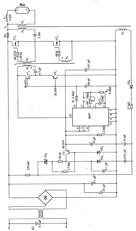
The circuit uses the separate excitation oscillation mode composed of 4047, the oscillation frequency is decided by Cll and R6.R (RP1). For high-speed drive power MOSFET (VT4 and VT5), it uses the buffer circuit composed of VT2 and VT3. Halogen lamp has 10 times difference between cold resistance and thermal resistance, therefore, when it gets power, it has a greater impulse current, which is more than 10 times of the steady-state current. Choke L1 can suppress this current below 1 / 3 times. Adjusting RP1 can change the oscillation frequency in order to do dimming.
(View)
View full Circuit Diagram | Comments | Reading(1658)
The drive circuit of metal halide lamp
Published:2011/7/4 23:28:00 Author:Lucas | Keyword: drive circuit , metal halide lamp

Output part is the the bridge circuit which is composed of the power MOSFET (VTl and VT2) and IGBT (VT3 and VT4). The bottom of the IGBT works in the switching frequency of (VT3 and VT4) 100Hz, then the electrode consumption of the metal halide lamp is the average current. The choking coil L2 keeps the current of lamp stable, but the top power MOSFET (VTl and VT2) works in the switching frequency of 41.67 k to make L2 lightweight. NE555 oscillates in the frequency of 100Hz, then the UC3842 detects the metal halide lamp current to generate 41.67 KHz PWM output pulse.
(View)
View full Circuit Diagram | Comments | Reading(1129)
Voltage / current conversion circuit composed of MPY634
Published:2011/7/5 6:44:00 Author:Lucas | Keyword: Voltage / current conversion
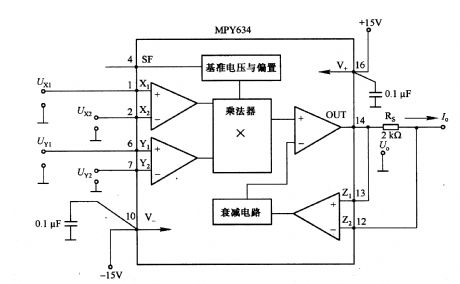
MPY634 is an analog multiplier with the output current being proportional to the product of two input signals X and Y (both AC and DC) . When the input is AC signal, it needs to use isolation transformer, which is not shown in the figure. Taking into account MPY634 computing precision, the maximum of output current is 5mA. Therefore, the output voltage U. Peak - peak value is lOV, the minimum of Rs is 2kΩ.
(View)
View full Circuit Diagram | Comments | Reading(1599)
Voltage / current conversion circuit composed of INA105
Published:2011/7/5 6:39:00 Author:Lucas | Keyword: Voltage / current conversion
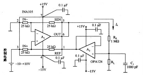
It can switch ±10V control voltage into ±lOμA tiny current. This circuit is used as small ion-current generator for chemical reaction. In the circuit, using A2 chip with resistor A1 (INA105) and low bias current operational amplifier A2 (OPA124) inside allows conversion accuracy in 0.1%. Output current prescribed minimum is decided by leakage current from the PCB and the ratio of the required output signal current and noise current. Accessing capacitor Cl can make effective value of noise circuit reduce from 317nA to 3.9 nA.
(View)
View full Circuit Diagram | Comments | Reading(668)
Sine wave converter circuit
Published:2011/7/5 8:04:00 Author:Lucas | Keyword: Sine wave converter
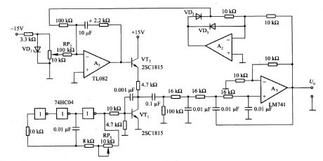
The circuit can be used as the signal source of calibration level meter or sensor-driven differential transformer. Circuit oscillation frequency is determined by the 74HCO4, and it is transferred lkHz by R. The supply voltage of Tl changes with the amplitude output. The switch turns the output voltage into square wave, then it will get sine wave by filtering the high frequency by low-pass filter. Waveform distortion depends on the performance of the filter, and the series of filter is used according to the need.
(View)
View full Circuit Diagram | Comments | Reading(2029)
Temperature/voltage conversion circuit of thermistor
Published:2011/7/5 7:57:00 Author:Lucas | Keyword: Temperature/voltage conversion, thermistor
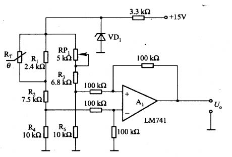
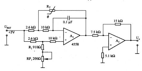
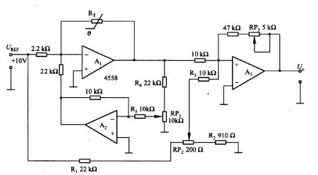
In the circuit shown in Figure 1-52 (a), Rl and thermistor RT are connected in parallel, and its role is to improve the linear relationship between the thermal resistor and temperature changing. RT and R1-R5 form a bridge with the bridge arm resistance in lOkΩ. Adjusting RP1 could keep the bridge balance, so that the output voltage is equal to zero at the required temperature. Output voltage U. is decided by the thermistor constant B and the voltage applied on bridge. Figure 1-52 (b) shows the circuit with the output voltage sensitivity in 1OmV / ℃, temperature measurement range in -50 +15 O ℃. When the bridge is added +5 V reference voltage U (REF), the thermistor RT will flow a constant current.
(View)
View full Circuit Diagram | Comments | Reading(4772)
Balance constant current output circuit
Published:2011/7/5 7:48:00 Author:Lucas | Keyword: Balance , constant current output
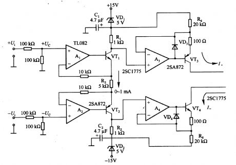
When the circuit has the external 0-10V voltage, you can choose a wide range of current, which is used as the part of the circuit of function generator, waveform generator. Al and A2 are the differential output circuit, which can change the unipolar input into a good balance circuit, and it can be used to change the 0-lOV input voltage into a 0-1mA output current. If Rl = R2, then the two ends of Rl, R2 will generat the same voltage, that is . It requires to generate the asymmetric waveform, so thatit need. It can also be used to generate a sawtooth waveform.
(View)
View full Circuit Diagram | Comments | Reading(2347)
| Pages:381/471 At 20381382383384385386387388389390391392393394395396397398399400Under 20 |
Circuit Categories
power supply circuit
Amplifier Circuit
Basic Circuit
LED and Light Circuit
Sensor Circuit
Signal Processing
Electrical Equipment Circuit
Control Circuit
Remote Control Circuit
A/D-D/A Converter Circuit
Audio Circuit
Measuring and Test Circuit
Communication Circuit
Computer-Related Circuit
555 Circuit
Automotive Circuit
Repairing Circuit