
Index
Cheap precision digital clock timing circuit
Published:2014/5/13 20:49:00 Author:lynne | Keyword: Cheap precision digital clock timing circuit, CD4060
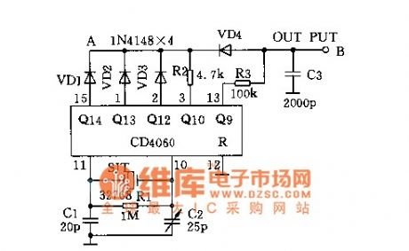
Cheap precision digital clock timing circuit shown as follow:
(View)
View full Circuit Diagram | Comments | Reading(3465)
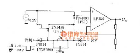
Auto device circuit diagram
Published:2014/4/22 21:21:00 Author:lynne | Keyword: Auto device circuit diagram
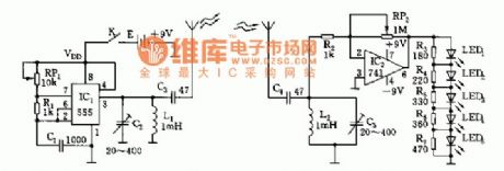
Auto device circuit diagram shown as follow:
(View)
View full Circuit Diagram | Comments | Reading(4852)
Cycle timer circuit diagram
Published:2014/4/22 21:22:00 Author:lynne | Keyword: Cycle timer circuit diagram
Cycle timer circuit diagram as shown:
(View)
View full Circuit Diagram | Comments | Reading(2582)
The car alarm circuit diagram
Published:2014/4/22 21:24:00 Author:lynne | Keyword: The car alarm circuit diagram
The car alarm circuit diagram shown as follow:
(View)
View full Circuit Diagram | Comments | Reading(2467)
Lights Timing Flashing Circuit Diagram
Published:2014/4/16 20:45:00 Author:lynne | Keyword: Lights Timing Flashing Circuit Diagram, 2N5060, MPU131
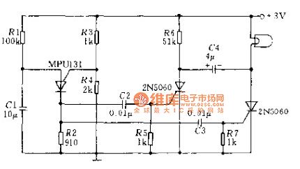
MPU131 thyristor is programmed with R1 and C1 class into relaxation oscillator circuit, the output control two-way thyristor 2N5060, thereby allowing low-voltage (2V) indicator lights timed flash.
(View)
View full Circuit Diagram | Comments | Reading(2072)
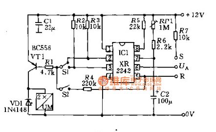
Timer switch circuit diagram
Published:2014/4/15 22:48:00 Author:lynne | Keyword: Timer switch circuit diagram, XR2242
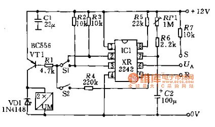
Monolithic circuit shown in FIG time transmitter circuit XR2242, timing time from a few milliseconds to a few days. The circuit comprises a time base oscillator, a binary counter 8 and a control trigger. Time base circuit by the resistor R and the capacitor C form, can have T = RC (pin 8). T = 2RC (pin 2) and T = 128RC (pin 3) three output pulse time by the applied voltage, the output can be reset automatically, use the flip-flop positive edge of the input pulse time can start the process. circuit output terminal (pin 6) voltage UA is low, so that the external action relays and other components. 6 may also be connected to the foot end of the R or S, the electric set or reset (switch S2 together). using the switch S1 can select the delay time. Timer switch circuit diagram shown in Figure:
(View)
View full Circuit Diagram | Comments | Reading(1957)
A/D conversion and liquid crystal display driver schematic circuit diagram
Published:2014/4/14 21:55:00 Author:lynne | Keyword: A/D conversion and liquid crystal display driver schematic circuit diagram
A / D converter 7106 is a double integral type A / D converter. The converter of high precision, it comes with the decoder output can directly drive an LCD display. 7106 LCD monitor is designed as a range of 200mV voltmeter. Portable electronic portable scale range is skg, 5kg load cell output when about 4.6mV. The picture shows the A / D converter and LCD driver schematic.
(View)
View full Circuit Diagram | Comments | Reading(2006)
MC1488 circuit diagram
Published:2014/4/7 21:33:00 Author:lynne | Keyword: MC1488 circuit diagram, MC1488
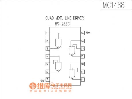
MC1488 circuit board as shown:
(View)
View full Circuit Diagram | Comments | Reading(2380)
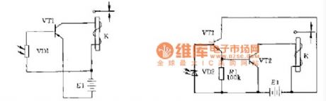
Light control switch circuit schematic
Published:2014/4/1 21:18:00 Author:lynne | Keyword: Light control switch circuit schematic
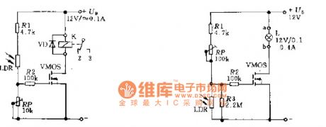
Using the sensor can be used for the power MOS FET power switch, the switch can be used photoresistor LDR. When light is irradiated onto the photosensitive resistor, LDR low resistance, a signal is applied to the gate of the field effect transistor off, the source and drain between conduction from the surface of the relay coil K changes state, for generating control signals, or, if connected to the photoresistor LDR at the low potential, in the dark when no light is irradiated onto the photosensitive resistor, with the photosensitive resistor. Light control switch circuit diagram shown in Fig.
(View)
View full Circuit Diagram | Comments | Reading(2247)
Infrared remote monitoring circuit schematic
Published:2014/4/1 21:17:00 Author:lynne | Keyword: Infrared remote monitoring circuit schematic
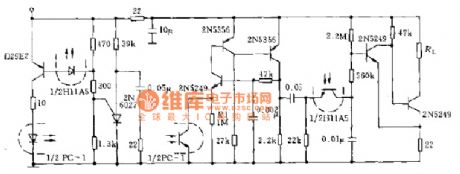
Infrared remote monitoring circuit schematic shown as follow:
(View)
View full Circuit Diagram | Comments | Reading(1967)
Switch Timing Circuit Diagram
Published:2014/3/31 21:33:00 Author:lynne | Keyword: Switch Timing Circuit Diagram
Switch Timing Circuit Diagram shown as follow:
(View)
View full Circuit Diagram | Comments | Reading(1793)
Light control relay circuit diagram
Published:2014/3/31 21:32:00 Author:lynne | Keyword: Light control relay circuit diagram
Light control relay circuit diagram as shown:
(View)
View full Circuit Diagram | Comments | Reading(2034)
Analog switch circuit schematic
Published:2014/3/31 21:31:00 Author:lynne | Keyword: Analog switch circuit schematic
Analog switch circuit schematic shown as follow:
(View)
View full Circuit Diagram | Comments | Reading(1780)
Loudspeaker overload protection circuit diagram
Published:2014/3/30 21:22:00 Author:lynne | Keyword: Loudspeaker overload protection circuit diagram
Loudspeaker overload protection circuit diagram shown as follow:
(View)
View full Circuit Diagram | Comments | Reading(2042)
Thyristor controlled motor reversing circuit diagram
Published:2014/3/30 21:07:00 Author:lynne | Keyword: Thyristor controlled motor reversing circuit diagram
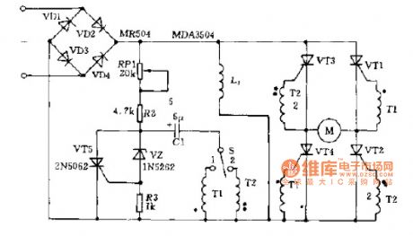
Thyristor controlled motor reversing circuit diagram shown as follow:
(View)
View full Circuit Diagram | Comments | Reading(2588)
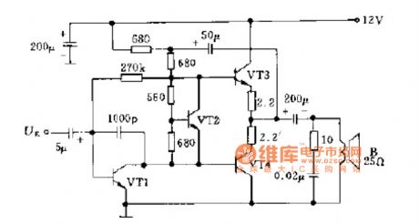
Fan controller circuit
Published:2014/3/26 21:44:00 Author:lynne | Keyword: Fan controller circuit
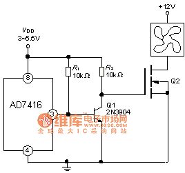
Fan controller circuit shown as follow:
(View)
View full Circuit Diagram | Comments | Reading(2736)
Transistor bistable trigger circuit diagram
Published:2014/3/24 21:29:00 Author:lynne | Keyword: Transistor bistable trigger circuit diagram
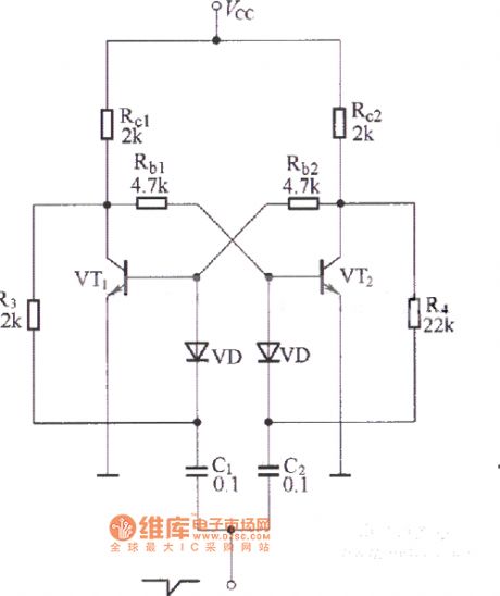
Transistor bistable trigger circuit diagram as shown:
(View)
View full Circuit Diagram | Comments | Reading(2342)
Blown fuse alarm circuit diagram
Published:2014/3/20 20:44:00 Author:lynne | Keyword: Blown fuse alarm circuit diagram, VT66A, 2CW52

With this alarm can quickly determine if the fuse blows .WorksFuse alarm circuit as shown. When the fuse Fu intact , Fu ends of the same potential , C1 voltage at both ends of days , the alarm does not work. When Fu blown fuse , 220V AC by the load ( ie, appliances ) input current limit by the Rl buck , VD2 rectifier , C1 filtering and VD1 regulated output DC voltage of about 3V . This DC voltage supply music IC VT66A work on piezoelectric ceramics B loud electronic music newspaper tube sound, alerting the master fuse has blown .Component selection and productionMusic IC available VT66A Music transistor should be used in L-shaped , with each song name within the reservoir favorite may be. VD1 with 2cw52 regulator diode , VD2 1N4004 type silicon rectifier diodes are available .R1 with RJ-1W metal film resistors. C1 with CD11-10v electrolytic capacitor . L color code available 2.5mH inductor . B with FT-27, HTD27A-1 type and other piezoelectric ceramics .Entire alarm lines can be installed in a small plastic box , leads to two wires , it will be parallel to the ends of the fuse Fu .As shown in Figure blown fuse alarm circuit diagram:
(View)
View full Circuit Diagram | Comments | Reading(1866)
Dongfeng Peugeot Citroen Picasso 2.0L sedan speeding alarm buzzer circuit diagram
Published:2014/3/17 21:39:00 Author:lynne | Keyword: Dongfeng Peugeot Citroen Picasso 2.0L sedan speeding alarm buzzer circuit diagram,
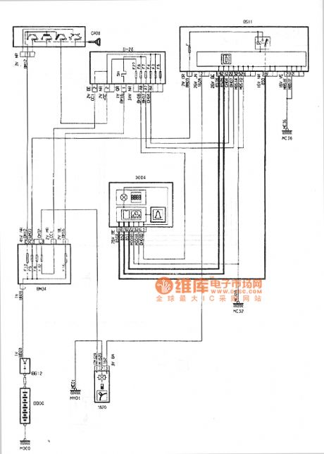
Dongfeng Peugeot Citroen Picasso 2.0L sedan speeding alarm buzzer circuit diagram as shown:
(View)
View full Circuit Diagram | Comments | Reading(1827)
The doppler effect and double control automatic door light socket (RD627) circuit
Published:2014/3/13 23:03:00 Author:lynne | Keyword: The doppler effect and double control automatic door light socket (RD627) circuit, RD627
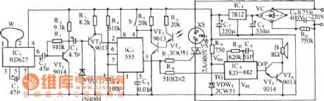
The circuit shown in FIG. It consists of the Doppler effect sensor head, light control switch, one-shot, SCR control circuit, vocal music buck rectifier circuit and the AC circuit. When a vehicle or pedestrian approached the front door, security door will open automatically, but will be broadcast on a melodious song. (View)
View full Circuit Diagram | Comments | Reading(2318)
| Pages:1/312 1234567891011121314151617181920Under 20 |
Circuit Categories
power supply circuit
Amplifier Circuit
Basic Circuit
LED and Light Circuit
Sensor Circuit
Signal Processing
Electrical Equipment Circuit
Control Circuit
Remote Control Circuit
A/D-D/A Converter Circuit
Audio Circuit
Measuring and Test Circuit
Communication Circuit
Computer-Related Circuit
555 Circuit
Automotive Circuit
Repairing Circuit