Other Circuit
Absorbing Capacitor Charging And Discharging Control Circuit
Published:2011/8/14 1:31:00 Author:Robert | Keyword: Absorbing, Capacitor, Charging, Discharging, Control | From:SeekIC
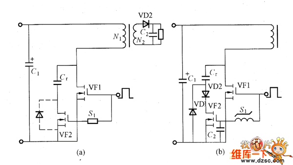
In the circuit shown in picture (a), VF1 is the primary side main MOSFET. The pulses from the PWM integrated controller can make it working in connected/disconnected mode. To make the VF2's connected/disconnected time be opposite to VF1, it adds the bidirectional time delay circuit S1. Now if the VF1 is in disconnected mode, the VF2 is in connected mode, the absorbing capacitor Cr would charge to the voltage between VF1's drain electrode and source electrode. So it also absorb the surge voltage on VF1. After the delay time, which is determined by the time delay circuit, the VF2 is disconnected. But at this time, the Cr two ports' voltage is equal to the voltage on VF1. So it is the zero-voltage and zero-current switching devices disconnected mode.
Reprinted Url Of This Article:
http://www.seekic.com/circuit_diagram/Electrical_Equipment_Circuit/Other_circuit/Absorbing_Capacitor_Charging_And_Discharging_Control_Circuit.html
Print this Page | Comments | Reading(3)

Article Categories
power supply circuit
Amplifier Circuit
Basic Circuit
LED and Light Circuit
Sensor Circuit
Signal Processing
Electrical Equipment Circuit
Control Circuit
Remote Control Circuit
A/D-D/A Converter Circuit
Audio Circuit
Measuring and Test Circuit
Communication Circuit
Computer-Related Circuit
555 Circuit
Automotive Circuit
Repairing Circuit
Code: