
Index 153
PRECISION_REFERENCE_BIPOLAR_OUTPUT_REFERENCE
Published:2009/7/1 2:39:00 Author:May
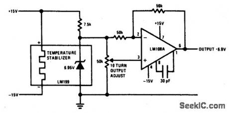
View full Circuit Diagram | Comments | Reading(521)
PRECISION_DUAL_TRACKING_VOLTAGE_REFERENCES
Published:2009/7/1 2:38:00 Author:May
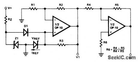
View full Circuit Diagram | Comments | Reading(593)
CONSTANT_CURRENT_SOURCE
Published:2009/7/1 2:38:00 Author:May
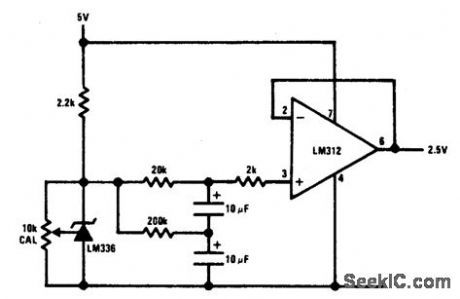
View full Circuit Diagram | Comments | Reading(1072)
Adjustable_step_up_converter
Published:2009/7/24 4:07:00 Author:Jessie
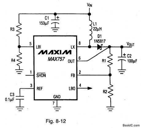
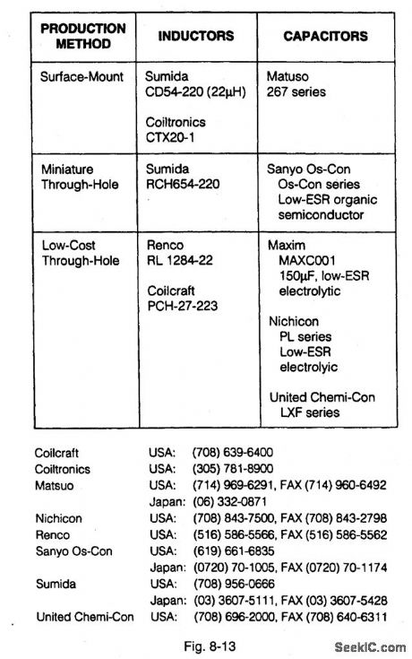
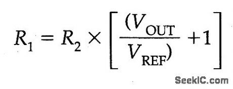
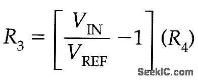
Figure 8-12 shows a MAX757 connected to provide an adjustable output from 2.7 V to 5.5 V, with a low-battery function. Figure 8-13 shows component suppliers. Let R2 be 100 kΩ, and select R1 for a desired output using:Where VREF is 1.25 V. Let R4 100 kΩ, and select R3for a desired threshold of the low-battery detector using:where VREF is 1.25V. MAXIM NEW RELEASES DATA BOOK, 1994. P. 4-178. (View)
View full Circuit Diagram | Comments | Reading(815)
Solid_state_circuit_breaker
Published:2009/7/24 4:18:00 Author:Jessie
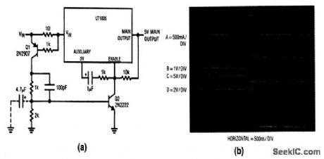
This circuit is the solid-state equivalent of a circuit breaker. The circuit turns off the main regulator output within 700 ns of an overload using the values shown. The trip current and breaker-delay point are settable over a wide range. Under normal operation, current through the 1-Ω shunt is insufficient to bias Q1 into conduction. Q2 is also off and the regulator produces an output. When an overload occurs (Trace A of Fig. 9-4B is the regulator output current), the potential across the 1-Ωresistor rises, turning on Q1. This drives the Q2 base (trace B), and turns Q2 on, grounding the enable pin (trace C) to shut down the regulator output (trace D). The 10-kΩ values from the main output to the pin latch the regulator down. The 1-Ω value can be changed to accommodate other desired current-trip points. The 4.7-μ.F capacitor (in dashed lines) can be added (delete the 100-pF capacitor) for applications where fast response is not desired. (View)
View full Circuit Diagram | Comments | Reading(954)
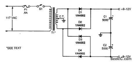
SIMPLE_DIGITAL_PANEL_METER_POWER_SOURCE
Published:2009/7/24 4:22:00 Author:Jessie
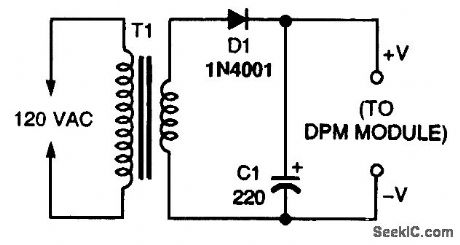
This source will supply 9 to 12 Vdc with floating ground, needed by many digital panel meters. (View)
View full Circuit Diagram | Comments | Reading(793)
Automatic_shutdown_for_abnormal_inputs110_V_220_V
Published:2009/7/24 4:20:00 Author:Jessie
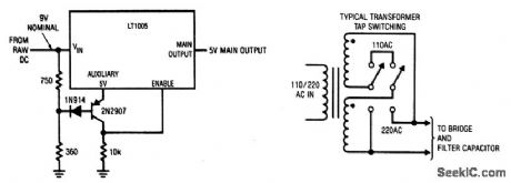
This circuit is useful in systems or instruments that can be powered from 110 V or 220 V (with a changeover switch). If a regulator is powered from 220 V with the switch set at 110 V, the regulator is forced to dissipate abnormal power, which causes thermal shutdown and possible damage. This circuit senses abnormally high input voltages and shuts down the regulator before thermal shutdown occurs. Normally, the input voltage is low enough to keep the transistor on, pulling the enable pin toward the auxiliary output and maintaining regulator output. If the circuit is inadvertently powered from 220 V, with the switch at 110V, VIN rises. This cuts off the transistor, and the 10-kΩ resistor pulls the enable pin to ground and shuts down the regulator. The diode prevents VBE from zenering during the reverse-bias condition, which exists during shutdown. For the values shown, the circuit functions over ranges of 88 to 135 Vac and 180 to 260 Vac (110 to 220 Vac ±20%). (View)
View full Circuit Diagram | Comments | Reading(577)
A_C_POWER_INTERLOCK
Published:2009/7/24 4:26:00 Author:Jessie
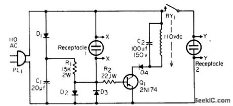
Any device drawing over 5 W (up to amount allowed by D2-D3) will produce 60-cps square wave at base of 01 when device is turned on, to energize relay through Q1 and apply power to receptacle 2.-C. J. Ulrick, AC Power Interlock, EEE, 13:6, p 65. (View)
View full Circuit Diagram | Comments | Reading(775)
Automatic_shutdown_during_power_outages
Published:2009/7/24 4:25:00 Author:Jessie
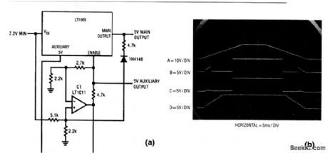
This circuit is useful when data bits must be transferred and stored into nonvolatile memory during power outages. The circuit takes advantage of the differing dropout voltages between the main and auxiliary outputs. When power is first applied, VIN (trace A in Fig. 9-6B) starts to rise (ramp up). The auxiliary output (trace D) follows this ramp action, and clamps at 5 V. During this interval, C1 monitors the difference between VIN and the 5-V auxiliary output. The resistor ratios are scaled so that the enable pin (trace B) is clamped until VIN is high enough to support main-output regulation. The small ramp segments that are visible at the enable pin are caused by the failure of C1 to clamp under a very low supply-voltage condition, and do not affect operation. The main output (trace C) comes up quickly. Because the auxiliary output precedes the main output, the auxiliary can be used to present conditions in the circuits being powered. When power falls below the threshold point, C1 pulls the enable pin low and forces the main output (trace C) off rapidly. However, the auxiliary output (trace D) maintains regulation after the main output is off. This allows the main output to be used as a logic signal to alert auxiliary-powered nonvolatile memory to store data. The amount of time that the auxiliary output will maintain regulation on power-down is controlled by the regulator tilter-capacitor size. The diode/4.7-kΩ combination provides regenerative action to ensure a clean turn-off for the main output. (View)
View full Circuit Diagram | Comments | Reading(554)
5_V_POWER_SUPPLY
Published:2009/7/24 4:23:00 Author:Jessie
The 5-V power supply shown here will provide voltage-regulated power for digital ICs needing up to 500 mA. With the 5-V power supply constructed as a separate unit, any circuit to be operated can be plugged in, and this allows it to provide power for various projects. It can also be used where a 5-Vdc, 500-mA supply is suitable, so it can, in some cases, be pressed into service where a 4.5- or 6-V battery would otherwise be fitted. (View)
View full Circuit Diagram | Comments | Reading(535)
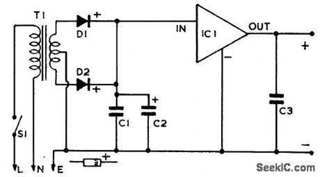
15_V_RECEIVER_POWER_SUPPLY_CHARGER
Published:2009/7/24 4:30:00 Author:Jessie
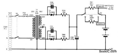
This power supply is for powering a receiver or similar load at 15 V, 100 mA. The NiCd battery pack is a 600-mAh AA cell assembly and is charged at 50 to 60 rnA. A 120-V primary transformer with the same secondary voltage can be substituted for the 230-V unit shown. (View)
View full Circuit Diagram | Comments | Reading(576)
HIGH_CURRENT_POWER_SUPPLY
Published:2009/7/24 4:29:00 Author:Jessie
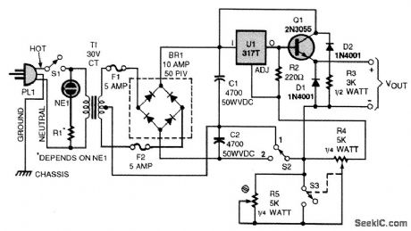
This 10-A power supply uses a 24- to 30-V center-tapped power transformer that is capable of delivering 5 to 10 A. The voltage output is controlled by the circuit consisting of R4, R5, and S3; note that S3 is part of R4. For a fixed-voltage output, R4 should be set for zero ohms (fully counterclockwise). In that position, switch 53, will open. Trimmer potentiometer R5 should then be adjusted so that the circuit produces a 12-V output (or whatever output your application demands). For an adjustable output, R4 is turned clockwise, closing S3, and removing R5 from the circuit. The output voltage is then controlled by the resistance offered by R4 alone. When SPDT switch S2 is in position 1, the maximum output current is achieved, with both halves of T1 providing current to the filter section to double the overall current output. However, the maximum output voltage is halved in that position. That is a more efficient setting because the power transistor need not drop as large a voltage. In position 2, the maximum voltage almost equals the rating of T1. D1 and D2 are included in case power is turned off with an inductive load attached. (View)
View full Circuit Diagram | Comments | Reading(1482)
DUAL_51_V_SWITCHING_POWER_SUPPLY
Published:2009/7/24 4:27:00 Author:Jessie
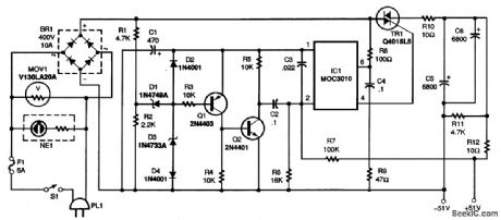
The ac voltage taken from PL1 feeds into bridge rectifier BR1, which delivers a full-wave output of approximately 165 Vdc.The network composed of R1, R2, D1, D3, and D4 generates a series of 5-V pulses that perform two important functions: First, the pulses are used as a 5-V power source for the pulse shaping and monostable network through D2 and C1. Second, the pulses trigger optoisolator IC1 and power triac TR1 via the pulse-shaping network, composed of Q1, Q2, and R3 to R5, and the mono-stable circuit, made of C2 and R6. Resistor R2 sets the maximum pulse width and, therefore, the maximum output voltage. With-out feedback, the unfiltered peak voltage is approximately 90 V. To obtain the required 51-V output, the feedback network (composed of R6, R7, and C3) reverse-biases the optoisolator whenever the output voltage exceeds 51 V. That, then forces TR1 Lo turn off as the unfiltered voltage goes to 0 V. The RC feedback network, therefore, regulates the output voltage by actively modifying IC1's conducting state. Resistor R8 limits the current through the optoisolator, and C4 and R9 ensure that the optoisolator's operation is stable and safe. Also, R10 limits surge current through TR1 when the supply is first turned on. Capacitors C5 and C6, along with R10, form a low-pass filter stage that minimizes ripple current. Resistor R11 discharges C5 and C6 when the power supply is turned off. (View)
View full Circuit Diagram | Comments | Reading(811)
Paralleling_three_terrninal_regulators
Published:2009/7/24 4:27:00 Author:Jessie
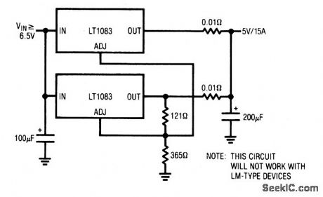
This circuit shows to use two three-terminal regulators to achieve and output current equal to the sum of the regulators. The circuit capitalizes on the 1 % output tolerance of the specified regulators to produce a simple parallel configu-ration. Both regulators sense from the same divider string. The series-output resistors provide ballast to account for the slightly differing output voltages. This added impedance degrades total drcuit regulation to about 1%. (View)
View full Circuit Diagram | Comments | Reading(1484)
Extending_three_terminal_regulator_current_capability_sznitch_mode
Published:2009/7/24 4:32:00 Author:Jessie

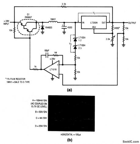
In this circuit, the LT350A functions in the normal manner and supplies a regulated output at 3-A capacity. The remaining components form a switch-mode dissipation-limiting control. This loop forces the potential across the LT350A to equal the 3.7-V value of VZ. When the input of the regulator (trace A, Fig. 9-9B) decays far enough, the LT1018 output (trace B) switches low and turns on Q1 (Q1 collector is trace D). This allows current flow (trace C) from the circuit input into the 4500-μF capacitor and raises the regulator input voltage. When the regulator input rises far enough, the comparator goes high, Q1 cuts off, and the capacitor ceases charging. Despite changes in input voltage, different regulated outputs or load shifts, the switch-mode loop ensures minimum possible dissipation in the regulator. (View)
View full Circuit Diagram | Comments | Reading(940)
SIMPLE_DUAL_VOLTAGE_POWER_SUPPLY
Published:2009/7/24 4:31:00 Author:Jessie
This circuit can be used to power op-amp circuits or other applications that require dual plus and minus supplies. This is a most basic circuit and is not regulated. T1 is a 120:12-V transformer of 100 mA (or more) capacity. (View)
View full Circuit Diagram | Comments | Reading(577)
Charge_pump_LCD_contrast_supply
Published:2009/7/24 5:30:00 Author:Jessie
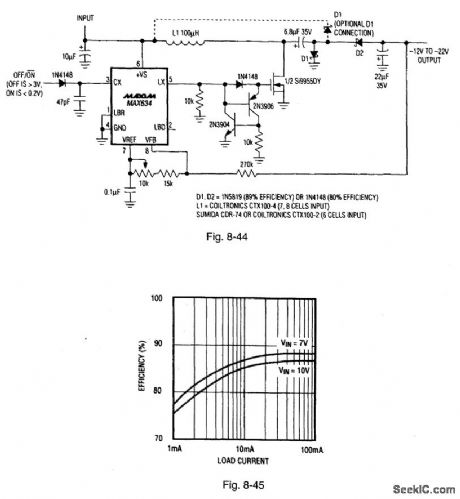
Figure 8-44 shows a MAX634 connected as an LCD-contrast supply using the charge-pump principle for higher efficiency. Figure 8-45 shows the efficiency curves. This circuit is particularly useful where the LCD supply must be operated directly from the battery. (The circuit is a hybrid in that the switching regulator boosts the input to a high positive output voltage, with the actual negative output voltage being generated by a charge-pump tap on the switching node.) The circuit operates over a 4-V to 16-V (four-to eight-cell) range, draws 330 μA of quiescent current, and is capable of a 30-mA output. The optional D1 connection (dotted line) is used when the battery voltage exceeds the absolute value of the output voltage. If this does not occur, connect D1 to ground. MAXIM BATTERY MANAGEMENT CIRCUIT COLLECTION, 1994, P. 49, 50.
(View)
View full Circuit Diagram | Comments | Reading(591)
Low_voltage_power_disconnect
Published:2009/7/24 5:29:00 Author:Jessie
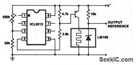
This circuit removes the power supply if the supply voltage drops below a certain value. As an example, the National Semiconductor LM199 precision reference has an on-chip heater that malfunctions with supply voltages below 9 V and it causes excessive device temperature. Using the values shown, the ICL8212 detects a supply voltage of 9 (or less) and turns off the supply to the LM199. (View)
View full Circuit Diagram | Comments | Reading(706)
Microporter_LCD_contrast_supply
Published:2009/7/24 5:28:00 Author:Jessie
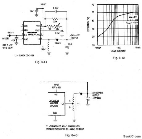
Figure 8-41 shows a MAX634 connected as a micropower LCD-contrast supply with an adjustable -5-V to -15-V output. Figure 8-42 shows the efficiency curve. This flea-power circuit is suitable for small multiplexed LCD displays (such as those on cellular phones). The circuit operates over a 4-V to 6-V range (with a maximum input/output differential of 24 V), draws 500-μA quiescent current, and is capable of 10-μA output. Figure 8-43 shows a way to extend the maximum input/output of 24-V by substituting an autotransformer for the inductor. MAXIM BATTERY MANAGEMENT CIRCUIT COLLECTION, 1994, P. 48.
(View)
View full Circuit Diagram | Comments | Reading(538)
Dc_dc_converter
Published:2009/7/24 5:28:00 Author:Jessie
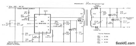
Although this circuit is designed to meet CCITT Standard 1.430 for ISDN (Integrated Services Digital Network) terminals, the circuit can be used for any battery-operated 15-V power-supply application. The input voltage is 22 to 42 V for maximum loads, and 30 to 42 V for minimum loads. Typical minimum loads are 3 mA at +5 V, and 0 mA at -5 V. Typical maximum loads are 100 mA at +5 V and 30 mA at -5 V. Ripple is 100 mV maximum at full load, and 60 mV typical at full load. Regulation is±5% typical and±7% worstcase. (View)
View full Circuit Diagram | Comments | Reading(0)
| Pages:153/291 At 20141142143144145146147148149150151152153154155156157158159160Under 20 |
Circuit Categories
power supply circuit
Amplifier Circuit
Basic Circuit
LED and Light Circuit
Sensor Circuit
Signal Processing
Electrical Equipment Circuit
Control Circuit
Remote Control Circuit
A/D-D/A Converter Circuit
Audio Circuit
Measuring and Test Circuit
Communication Circuit
Computer-Related Circuit
555 Circuit
Automotive Circuit
Repairing Circuit