
Index 155
High_supply_voltage_dump_circuit
Published:2009/7/24 5:21:00 Author:Jessie
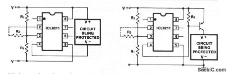
These circuits remove the power supply when there is a high-voltage overload. For circuits consuming less than 5 mA, the ICL8211 can drive the load directly. For higher load currents, a pnp or Darlington pair is required as shown. Resistors R1 and R2 set up the disconnect voltage, and R3 provides optional voltage hysteresis. (View)
View full Circuit Diagram | Comments | Reading(709)
CCFT_CCFL_backlight_supplies
Published:2009/7/24 5:21:00 Author:Jessie
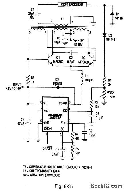
Figure 8-35 shows a MAX752 connected as a power supply for cold-cathode fluorescent tubes (CCFT or CCFL, whichever you prefer). CCFT/CCFLs require high-voltage aqpower, taken from a source that is not part of the main power supply. This is because the supply should be located physically close to the display (to prevent losses resulting from cable capacitance). Typically, the CCFT/CCFLs need about 2 W of 400-Vac power (that must reach near 1200 V upon startup) to arc and turn on the lamp. In this circuit, the MAX752 boost-regulator IC acts as a switching-regulator current source to feed the tail of a traditional Royer-type self-oscillating dc/dc converter. The Royer circuit drives a 33:1 transformer that steps up the battery voltage to ac high voltages (near 1200 V). Capacitance C2 and the primary inductance form a resonant circuit, which provides a low-EMI sine-wave drive signal to the lamp. A half-wave rectified signal proportional to tube current is returned to the MAX752 feedback input. This maintains the CCFT/CCFL current at a constant level. Display brightness is adjusted by R2. MAXIM ENGINEERING JOURNAL, Vot. 3, 1994, P. 51. (View)
View full Circuit Diagram | Comments | Reading(1890)
Strobed_power_strain_gauge_bridge
Published:2009/7/24 5:19:00 Author:Jessie
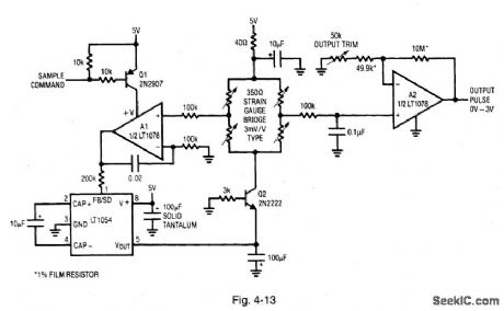
Figure 4-13 (derived from Fig. 4-6) shows a way to reduce power without sacrificing bridge signal-output level. The technique is applicable where continuous output is not a requirement. The circuit is in a quiescent state for long periods with relatively brief on times. (A typical application would be where remote weight information in storage tanks is sampled once per week.) Quiescent current is about 150 μA, with on-state current typically 50 mA. LINEAR TECHNOLOGY, APPLICATION NOTE 43, P. 19. (View)
View full Circuit Diagram | Comments | Reading(650)
High_stability_voltage_reference
Published:2009/7/24 5:15:00 Author:Jessie
This circuit provides a precision voltage reference without the use of an IC voltage reference. (View)
View full Circuit Diagram | Comments | Reading(1179)
Thermally_based_NiCad_charger_with_low_imynedance_charging_source
Published:2009/7/24 5:15:00 Author:Jessie
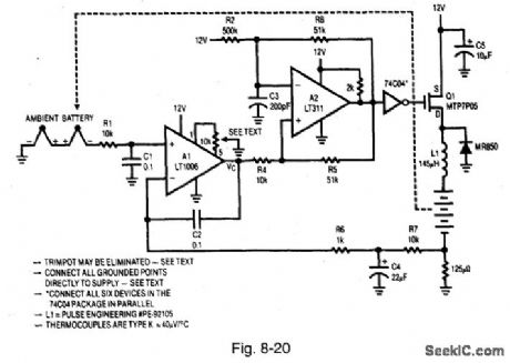
Figure 8-19 shows a thermally based NiCad charger operated in the switching mode. The circuits of Figs. 8-15 and 8-18 both force the transistor to dissipate some power, and the resulting heat might be a problem in a small enclosure (typical of micropower circuits). The circuit of Fig. 8-19 relies on the source impedance of the wall transformer to limit current through Q1 and the battery pack. The source impedance can be set when specifying the transformer. LINEAR TECHNQLOGY, APPLICATION NOTE 37, P. 3. (View)
View full Circuit Diagram | Comments | Reading(498)
ac_power_fail_and_brownout_detector
Published:2009/7/24 5:08:00 Author:Jessie
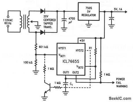
This circuit detects ac undervoltage by monitoring the secondary side of the transformer with an ICL7665S(Fig.9-15B).C1 is charged through R1 when OUT1 is off.With a nominal 110 V input to the transformer,OUT1 discharges C1once every cycle(about every 16.7 ms).When the ac input voltage is reduced,OUT1 stays off so that C1 does not discharge.When the voltage on C1 reaches 1.3V,OUT2 turns off,and the power-fail warning goes high.The R1C1 time constant is chosen so that it takes longer than 16.7 ms to charge C1 to 1.3 V. (View)
View full Circuit Diagram | Comments | Reading(1298)
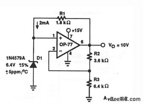
ZENERLESS_PRECISION_MILIVOLT_SOURCE
Published:2009/7/1 2:22:00 Author:May
View full Circuit Diagram | Comments | Reading(624)
Power_fail_warning_and_power_up_power_down_reset
Published:2009/7/24 5:01:00 Author:Jessie
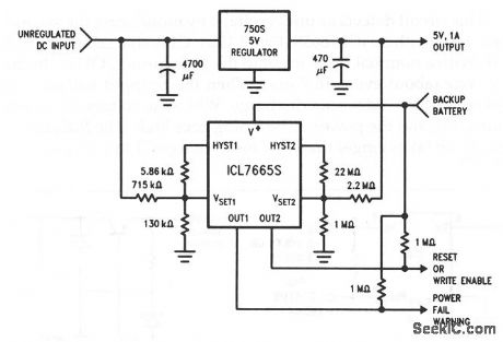
When the unregulated dc input of this circuit is above the trip point, OUT1 is low. When the dc input drops below the trip point, OUT1 shuts off and the power-fail warning goes high. The voltage on the input of the 7805 decays at a rate of IOUT/C. Because the 7805 continues to provide a 5-V output at 1 A until VIN is less than 7.3v, this circuit provides a certain amount of warning before the 5-V output begins to drop. The ICL7665S OUT2 (Fig. 9-15B) is used to prevent a microprocessor from writing spurious data to a CMOS battery-backup memory by causing OUT2 to go low when the 7805 5-V output drops below the ICL7665S trip point. (View)
View full Circuit Diagram | Comments | Reading(1106)
Multiple_supply_fault_monitor
Published:2009/7/24 4:57:00 Author:Jessie
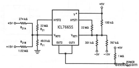
This circuit shows an overvoltage/undervoltage fault monitor for multiple supplies, using a single ICL7665S detector. Figure 9-15B shows the pin connections. The resistors are chosen such that the sum of the currents through R21A, R21B and R31 is equal to the current through R11 when the two input voltages are at the desired low-voltage detection point. The current through R11 at this point is equal to 1.3 V/R11. The voltage at the VSET input depends on the voltage of both supplies being monitored. The trip voltage of one supply (while the other supply is at the nominal voltage) will be different than the trip voltages when both supplies are below their normal voltages. The other side of the ICL7665S can be used to detect the absence of negative supplies. The trip points for OUT1 depend on both the negative supply voltages and the actual voltage of the +5-V supply. (View)
View full Circuit Diagram | Comments | Reading(648)
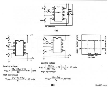
Nonvolatile_low_voltage_indicator
Published:2009/7/24 5:15:00 Author:Jessie
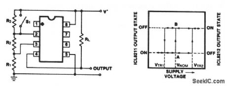
In this circuit, the high-trip voltage VTR2 is set above the normal supply-voltage range. On power-up, the initial condition is A. When S1 is closed momentarily, the operating point changes to B, and remains at B until the supply voltage drops below VTR1, at which time the output reverts to A. Notice that state A is always retained if the supply voltage is reduced below VTR1 (even to 0 V) and then raised back to VNOM. Figure 9-21B shows the equations to calculate resistor values. (View)
View full Circuit Diagram | Comments | Reading(484)
Linearized_platinum_RTD_resistance_bridge
Published:2009/7/24 5:14:00 Author:Jessie
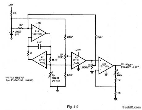
Figure 4-9 shows a bridge with a ground-referred RTD to Improve noise rejection,The RTD leg is driven by a current Source, with the opposite bridge branch voltage biased.The current drive allows the bridge voltage across the RTD to vary directly with the temperature-induced resistance shift. The difference between this potential and that of the opposing bridge leg forms the bridge output,To calibrate, substitute a precision decade box(General Radio 1432k)for RP. Set the box to the0℃ value(100.00Ω)and adjust the offset trim for a 0.00-V output. Then set the decade box for a 140℃ output(154.26Ω)and adjust the gain trim for a 3.500-V output reading, Finally, set the box to 249.0V-Ω(400.00℃)and trim the linearity adjustment for a 10.000-V output. Repeat the sequence until all three points are fixed.The total error over the entire range will be within ±0.05℃. The resistance values given are for a nominal 100.00 Ω(0℃)sensor. Sensors deviating from this nominal value can be used by factoring In the deviation from 100.00Ω.LINEARTECHNOLOGY,APPLICATION NOTE 43,P. 11. (View)
View full Circuit Diagram | Comments | Reading(614)
Switch_mode_thermally_based_NiCad_charger
Published:2009/7/24 5:13:00 Author:Jessie
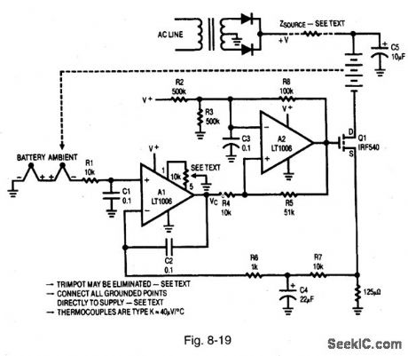
Figure 8-19 shows a thermally based NiCad charger operated in the switching mode. The circuits of Figs. 8-15 and 8-18 both force the transistor to dissipate some power, and the resulting heat might be a problem in a small enclosure (typical of micropower circuits). The circuit of Fig. 8-19 relies on the source impedance of the wall transformer to limit current through Q1 and the battery pack. The source impedance can be set when specifying the transformer. LINEAR TECHNQLOGY, APPLICATION NOTE 37, P. 3. (View)
View full Circuit Diagram | Comments | Reading(758)
Floating_input_bridge
Published:2009/7/24 5:12:00 Author:Jessie

Figure 4-8 shows an optically coupled switched-capacitor bridge with a floating input. The common-mode rejection ratio at dc for the front-end exceeds 160 dB. The amplifier operates over a ±200-V common-mode range. Gain-accuracy and stability are limited only by external resistors. The offset drift is 0.05-μV/℃. The optical drive to the MOSFET eliminates the charge-injection problems that are common to FET switched-capacitor networks. LINEAR TECHNOLOGY, APPLICATION NOTE 43, P, 10. (View)
View full Circuit Diagram | Comments | Reading(671)
Low_voltage_battery_indicator_
Published:2009/7/24 5:12:00 Author:Jessie
This application is particularly suitable for portable or remotely operated equipment, which requires an indication of a depleted or discharged battery. The quiescent current is typically 35 μA, which increases to 7 mA when the LED is turned on. R3 is optional and provides hysteresis if desired. Figure 9-21B shows the equations to calculate resistor values. (View)
View full Circuit Diagram | Comments | Reading(747)
NiCad_charger_for_grounded_batteries
Published:2009/7/24 5:12:00 Author:Jessie
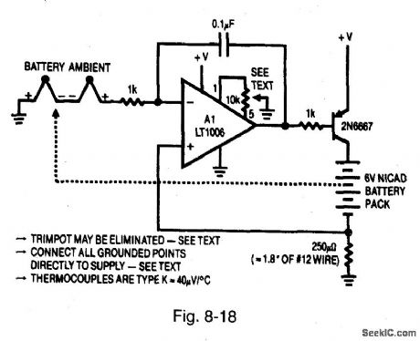
Figure 8-18 showp a thermally based NiCad charger for use with batteries that are common to ground. The transistor is connected as a common emitter, so the inputs to A1 are reversed. However, operation is the same as for the Fig. 8-15 circuit. Notice that in both the Fig. 8-15 and 8-18 circuits, the trimpot can be eliminated by specifying an LT1006 set (at manufacture) to the desired offset value. High-quality grounds must be used, and all ground returns must be brought directly back to the supply common terminal. LINEAR TECHNOLOGY, APPLICATION NOTE 37, PAGE 2.
(View)
View full Circuit Diagram | Comments | Reading(599)
Thermally_based_NiCad_charger
Published:2009/7/24 5:10:00 Author:Jessie

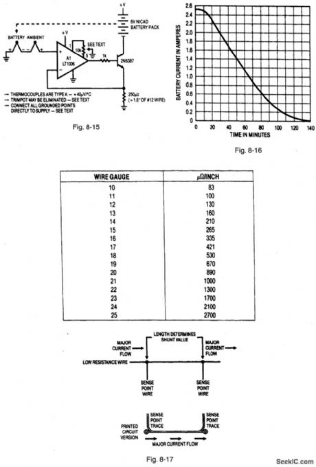
Figure 8-15 shows a simple thermally based charging circuit for NiCad batteries.Figure 8-16 shows the charge characteristics.Thermocouples sense both cell andambient temperature simultaneously. A1 provides the amplification necessary for microvolt-level thermocouple signals. The 10-kΩ trimpot is set to introduceenough input-off set so that the A1 output swmgs positive turning on thetransistor. Figure 8-17 shows a simple, lnexpenslve way to construct low-resistance shunts usmg a small length of wlre or a PC trace.The type and length of wire determines the shunt resistance (which can be altered to produce the desiredcharging characteristics). Figure 8-17 also shows resistance-versus-len gth characteristics for varlous wire sizes, as well as the details for both wlre and PC shunts.In both cases (PC or wire) the shunt should have separate connections for sensing (Kelvin style) SO that high current does not affect the readings.LINEARTECHNOLOGY, APPLICATION NOTE 37.P.4. (View)
View full Circuit Diagram | Comments | Reading(533)
IC_battery_backup_rechargeable_battery
Published:2009/7/24 5:10:00 Author:Jessie
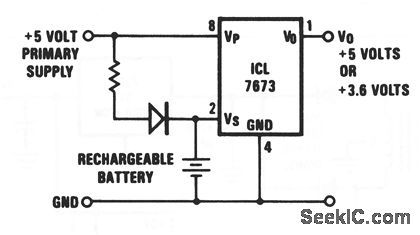
This circuit is similar to that of Fig.9-19,except that a trickle charge is applied to a rechargeable battery(through the diode and resistor). (View)
View full Circuit Diagram | Comments | Reading(796)
NONINVERTING_BIPOLAR_CURRENT_SOURCE
Published:2009/7/1 2:07:00 Author:May
View full Circuit Diagram | Comments | Reading(585)
LOW_VOLTAGE_ADJUSTABLE_REFERENCE_SUPPLY
Published:2009/7/1 2:07:00 Author:May
View full Circuit Diagram | Comments | Reading(548)
IC_battery_backup_lithium_battery
Published:2009/7/24 5:09:00 Author:Jessie
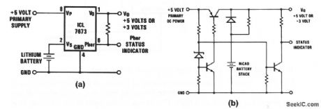
The circuit of Fig.9-19A uses single ICL7873 to replace a typical discrete-component battery-backup system, such as shown in Fig. 9-19B. (View)
View full Circuit Diagram | Comments | Reading(1501)
| Pages:155/291 At 20141142143144145146147148149150151152153154155156157158159160Under 20 |
Circuit Categories
power supply circuit
Amplifier Circuit
Basic Circuit
LED and Light Circuit
Sensor Circuit
Signal Processing
Electrical Equipment Circuit
Control Circuit
Remote Control Circuit
A/D-D/A Converter Circuit
Audio Circuit
Measuring and Test Circuit
Communication Circuit
Computer-Related Circuit
555 Circuit
Automotive Circuit
Repairing Circuit