
Index 158
Regulated_power_distribution_system
Published:2009/7/24 8:38:00 Author:Jessie
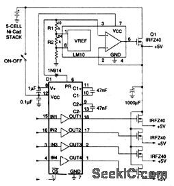
In this circuit, the LM10 linear regulator provides a maximum dropout voltage (at 25℃) of less than 90 mV at 5 A when used with a low-resistance MOSFET (such as an SMP60N06-18). The load switches are driven by the high-side voltage, which is regulated at + 11V above the supply voltage, via the four on-board latched-level translators. (View)
View full Circuit Diagram | Comments | Reading(831)
Full_function_portable_power
Published:2009/7/24 8:37:00 Author:Jessie
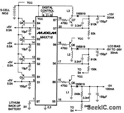
This circuit provides a variety of outputs for battery-operated micro-processor systems. All of the outputs are under microprocessor control. A 5-cell NiCd battery is used for the main power source, with a 3-V lithium back-up battery One of the outputs is negative (and is controlled by a 5-bit on-board D/A converter) for LCD contrast adjustment. (View)
View full Circuit Diagram | Comments | Reading(570)
Battery_input_buck_boost_regulator
Published:2009/7/24 8:36:00 Author:Jessie
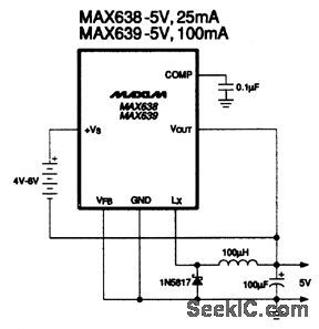
This circuit converts an input voltage that can range from above (6 V) and below (4 V) the desired output voltage (5 V). Normally, such a circuit must provide both step-up and step-down actions. However, if the input ground can be floated, as is often the case with a battery, an inverter can be used instead of a transformer or a complicated and lossy step-up/down circuit by fixing the most-negative output voltage at ground. (View)
View full Circuit Diagram | Comments | Reading(578)
Step_up__5_V_output_from_two_AA_cells
Published:2009/7/24 8:35:00 Author:Jessie
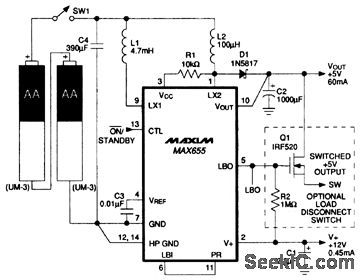
In this circuit, a MAX655 provides a +5-V 60-mA output from two AA battery cells. The circuit also provides a +12-V 500-μA output. Notice that the low-battery detector (LBO) is used as a level translator for optional high-side switching. Standby current is 80μA (with the +5-V output still alive and regulating) and efficiency is 82%. (View)
View full Circuit Diagram | Comments | Reading(551)
Cold_cathode_fluorescent_lamp_CCFL_power_supply
Published:2009/7/24 8:24:00 Author:Jessie
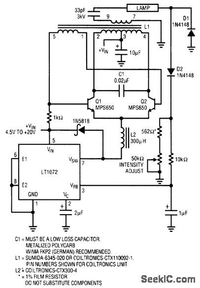
CCFLs are often used to backlight the LCD displays of portable computers. Such lamps require a high-voltage sine-wave drive. This circuit provides such drive,and permits lamp intensity to be varied continuously and smoothly from zero to full intensity. Notice that a Tektronix probe type P-6009(acceptable)or types P6013A and P6015(preferred)probes must be used to read the L1 output,The vast majority of oscilloscope probes will break down if used for this measurement,unless the probes are rated for wideband high voltage (View)
View full Circuit Diagram | Comments | Reading(751)
Regulators_with_ultra_low_dropout
Published:2009/7/24 8:22:00 Author:Jessie
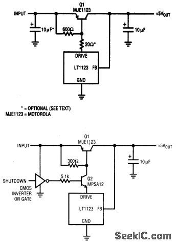
Battery life is significantly affected by the dropout performance of linear regulators. These circuits offer lower dropout voltage than any monolithic regulator (below 50 mV at 1 A, increasing to only 450 mA at 5 A). Line and load regulation are within 5 mV, and initial output accuracy is inside 1%. The circuits are fully short-circuit protected, and have no-load quiescent current of 600μA. Figure 4-37B shows a simple way to add shutdown to the regulator of Fig. 4-37A.A CMOS inverter or gate biases Q2 to control LT1123 bias. When Q2 is driven, the loop functions normally. With Q2 unbiased, the circuit goes into shutdown and pulls no current. (View)
View full Circuit Diagram | Comments | Reading(785)
Simple_voltage_programmable_current_source
Published:2009/7/24 8:21:00 Author:Jessie
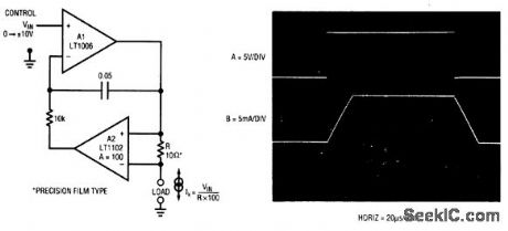
This circuit produces output current in strict accordance with the sign and magnitude of the control voltage, with no trimming required. Circuit accuracy and stability depend almost entirely on resistor R. Figure 4-36B shows dynamic response for a full-scale input step. Trace A is the voltage-control input and trace B shows the output current. (View)
View full Circuit Diagram | Comments | Reading(688)
Series_resonant_power_supply
Published:2009/7/24 8:20:00 Author:Jessie
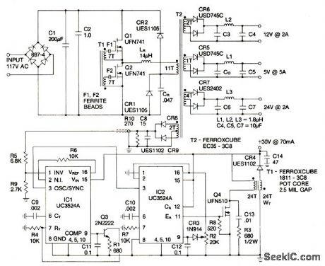
The advantages of a series-resonant converter, compared to a buck-derived switching regulator, are higher overall efficiency, smaller weight and volume, reduction in EMI, and increased reliability. The disadvantages are: an additional resonant circuit, the rating of the power switch is about 1.4 times higher, and the output filter capacitors must have low ESR and high ripple-current ratings. (View)
View full Circuit Diagram | Comments | Reading(1239)
High_frequency_switching_regulator
Published:2009/7/24 8:17:00 Author:Jessie

Because of their fast switching time, low-voltage hybrid circuits (such as the PIC600) can be operated as high as 250 kHz. The advantages of the higher frequencies are: lower filter cost, reduced size and weight, improved transient response, output ripple less dependent on capacitor ESR, and simpler EMI and RFI filtering. (View)
View full Circuit Diagram | Comments | Reading(1369)
HIGH_POWER_BATTERY_OPERATED_FLASHER
Published:2009/6/30 22:46:00 Author:May
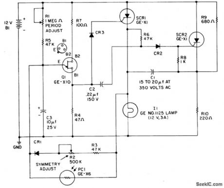
This flasher operates from a 12-volt car or boat battery. It offers 36 to 40-watts output, variable flash rate (up to 60 flashes per minute), independent control of both on and off cycles and photoelectric night and day control that turns the flasher on at night and shuts it off during the day for automatic operation. SCR1 and SCR2 form a basic dc flip-flop. The lamp load is the cathode leg of one SCR so that the other side of the load may be at ground (negative) potential (required in some applications). The flip-flop timing is controlled by a conventional UJT oscillator arrangement (Q1, R1, C3, etc.). Potentiometer R2 and diode CR1 provide on/off timing independence. Photoconductor PC1 locks out the UJT firing circuit during the daylight hours. (View)
View full Circuit Diagram | Comments | Reading(539)
5_V_to_isolated_5_V_at_20_mA
Published:2009/7/24 9:08:00 Author:Jessie
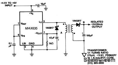
In this circuit, a negative-output dc/dc converter generates a -5-V output at point A. To generate this -5 V at A, the transformer primary must flyback to a diode drop that is more negative than -5 V. If the transformer has a tightly-coupled 1:1 turns ratio, 5 V (plus a diode drop) is across the secondary. The 1N5817 rectifies this secondary voltage to generate an isolated 5-V output (which is not fully regulated because the -5 V at point A is sensed by the MAX635). With careful transformer selection, the 5-V output will be within 10%. Bifilar winding of the transformer provides better load regulation of the isolated 5-V output, but this does reduce the isolation by increasing the capacitance between the primary and secondary. The isolation voltage breakdown is determined by the characteristics of the transformer, not the MAX635. (View)
View full Circuit Diagram | Comments | Reading(554)
Isolated__15_V_dc_dc_converter
Published:2009/7/24 9:07:00 Author:Jessie
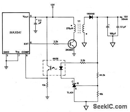
In this circuit, a TL431 shunt regulator is used to sense the output voltage. The TL431 drives the LED of a 4N28 optocoupler, which provides feedback to the MAX641 while maintaining isolation between the + 12-V input and the +15-V output (which is fully regulated with respect to both line and load changes). (View)
View full Circuit Diagram | Comments | Reading(2267)
RS_232_line_to_5_V
Published:2009/7/24 9:05:00 Author:Jessie
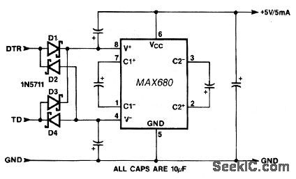
The MAX680 is normally used as a charge-pump voltage converter which converts +5 V to± 10V. In this circuit, the MAX680 works in reverse, and converts the RS-232 signal levels to a lower voltage. When the RS-232 inputs are driven by 1488 drivers powered by±12V, the output voltage varies from 5.3 V open-circuit to 4-5 V with a 5-mA output load. (View)
View full Circuit Diagram | Comments | Reading(573)
Telecom__48_to_5_V_at_05_A
Published:2009/7/24 9:04:00 Author:Jessie
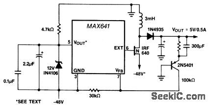
The small current consumption of a MAX641 allows the IC to be biased at a -50-V rail with a shunt zener so that the IC can convert -50 to +5 V. This is a common requirement in telecom systems, where logic circuits must be powered from the central-office battery voltage. A small high-voltage pnp level-shifts the feedback signal from the + 5-V output down to the pin MAX641, where the ground pin is tied to the 50-V input (instead of true ground). This is done so that EXT can drive the MOSFET to switch the inductor to -50 V, making the circuit operate similar to a step-up dc/dc converter. The 330-pF capacitor provides feed-forward compensation to stabilize the regulator control loop. (View)
View full Circuit Diagram | Comments | Reading(742)
3_state_battery_indicator
Published:2009/7/24 9:15:00 Author:Jessie
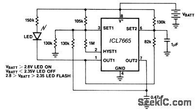
This circuit shows the state of a battery (typically 3V) by means of an LED and an ICL7665, The LED remains on if the battery voltage is above 2.8 V, and flashes if the battery voltage is between 2.35 and 2.8 V. The LED remains off if the battery voltage drops below 2.35V. (View)
View full Circuit Diagram | Comments | Reading(1477)
Precision_voltage_regulrttor_controller
Published:2009/7/24 20:10:00 Author:Jessie
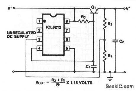
In this circuit, the ICL8212 is used as the controller for a highly-stable series voltage regulator. The output voltage is simply programmed, using resistor divider network R1/R2. C1 and C2 are required to ensure stability because the ICL8212 is not compensated internally. This regulator system can be used with lower input voltages and it consumes less power for a given output control current than most commercial regulators. Thus, the circuit is most useful for battery-powered systems that operate at low voltages. (View)
View full Circuit Diagram | Comments | Reading(614)
Constant_current_source
Published:2009/7/24 20:08:00 Author:Jessie
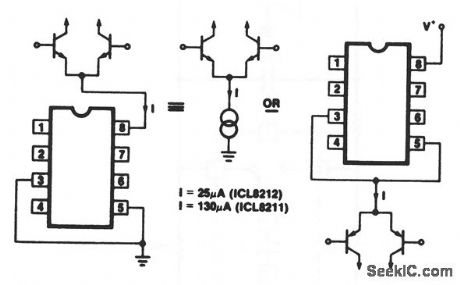
The ICL8212 and ICL8211 provide constant current sources of 25 and 130 μA, respectively, when connected as shown. The equivalent parallel resistance is in the tens of megohms over the supply-voltage range from 2 to 30 V. (View)
View full Circuit Diagram | Comments | Reading(1)
Programmable_Zener_voltage_reference
Published:2009/7/24 20:07:00 Author:Jessie


In this circuit, an ICL8212 stimulates a Zener diode by connecting the output terminal (pin 4) to the VZ output, and using a resistor network connected at the VTH terminal (pin 3) to program the Zener voltage. Power (V+) is applied to pin 8, with pin 5 connected to ground. The zener voltage is calculated by:
Because there is no internal compensation, the 5-μF capacitor is required across the output to prevent oscillation. Zener voltages from 2 to 30 V can be programmed. Typical impedance values between 300 μA and 25 mA range from 4 to 7Ω. The Zener knee is sharper and occurs at a significantly lower current than similar devices. (View)
View full Circuit Diagram | Comments | Reading(653)
Op_amp_pulse_width_modulator
Published:2009/7/24 21:37:00 Author:Jessie
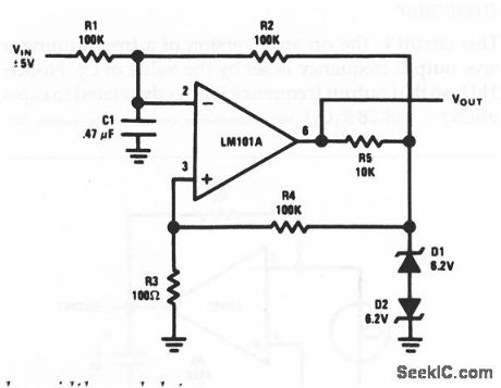
This circuit is similar to that of Fig. 10-21, except that the duty cycle of the output is controlled by VIN. (View)
View full Circuit Diagram | Comments | Reading(582)
Integrator_with_bias_current_compensation
Published:2009/7/24 21:27:00 Author:Jessie
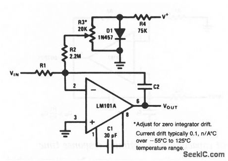
This circuit is similar to that of Fig. 10-10, except that the input bias current can be adjusted for zero drift. (View)
View full Circuit Diagram | Comments | Reading(1205)
| Pages:158/291 At 20141142143144145146147148149150151152153154155156157158159160Under 20 |
Circuit Categories
power supply circuit
Amplifier Circuit
Basic Circuit
LED and Light Circuit
Sensor Circuit
Signal Processing
Electrical Equipment Circuit
Control Circuit
Remote Control Circuit
A/D-D/A Converter Circuit
Audio Circuit
Measuring and Test Circuit
Communication Circuit
Computer-Related Circuit
555 Circuit
Automotive Circuit
Repairing Circuit