
Index 163
Automatic charger circuit diagram
Published:2011/7/25 0:11:00 Author:Sophia | Keyword: Automatic charger
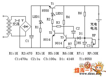
Circuit theory
The circuit is designed aiming at a single-cell Ni-MH battery. Figure: electricity is transformed through the transformer and rectified by full-bridge. Capacitor C1 is filtered into DC. LED1 is the power indicator, LED2 is the charge indicator. T1 is the charge control transistor, which works in the switch state; T2, T3 and C2 constitute a monostable flip-flop. R6 and RP constitute a limited pressure sampling circuit. R7 is limiting the sampling resistor.
Standby: the power must be on, if not, transistor T2 will be cut-off because of no base voltage, and transistor T1 is also closed, no voltage is outputed. At this moment, only the power indicator LED1 lights.
(View)
View full Circuit Diagram | Comments | Reading(1343)
Switching_regulator_using_a_timer
Published:2009/7/25 0:21:00 Author:Jessie
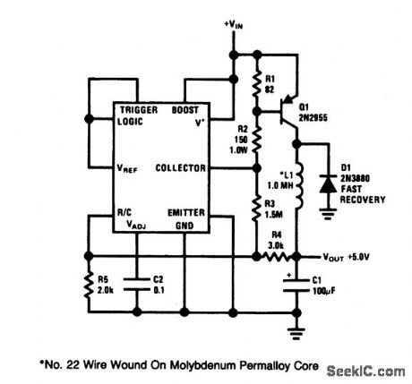
This circuit uses an LM122 timer to provide switching regulation. (The internal reference and comparator of the timer are used to drive a pnp switch transistor). Circuit features include a 5.5-V minimum input voltage at 1-A output current, low parts count, and good efficiency (greater than 75% ) for input voltages up to 10 V. Output ripple at the switching frequency is about 30 mV. Other values for Vout can be obtained with corresponding values of R2, R3, R4, and R5. (View)
View full Circuit Diagram | Comments | Reading(552)
The function circuit of bootstrap circuit
Published:2011/7/29 2:36:00 Author:Sophia | Keyword: bootstrap circuit, function
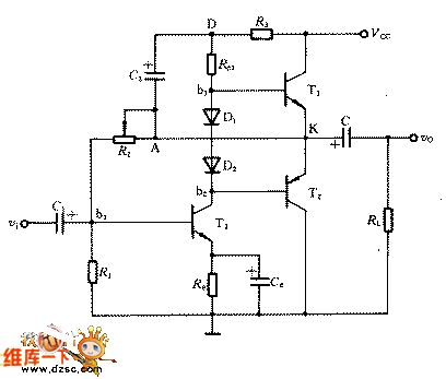
The function of bootstrap circuit
When the circuit is in the static state, , when R3C3 is large enough,VC3doesn't change with vi, actually has no change. So when vi is negative, T1 conducts the electricity,vKwill change from VCC/2 to correct direction. Considering vD=vC3+vK= VC3+vK, obviously, with the rise of electric potential of K spot, D spot electric potential vD will rise automatically. So even if the output voltage amplitude rise very highly, there are enough current iB1 to make theT1 fully conductive. This working is called the bootstrap, which means the circuit itself increase vD.
(View)
View full Circuit Diagram | Comments | Reading(1050)
Low_current_ammeter
Published:2009/7/25 0:11:00 Author:Jessie
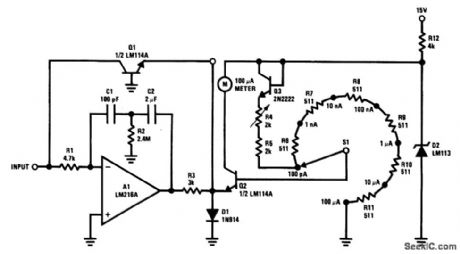
This classic circuit can be updated by substituting an LM11 for the LM216A, an LM194 for the LM114A, and an LM185-1.2 for the LM113. To calibrate, apply a 1-μA input current, and adjust R4 for a full-scale deflection of the 100-μA meter (with S1 set to 1μA). (View)
View full Circuit Diagram | Comments | Reading(1667)
Fast_ac_dc_converter
Published:2009/7/25 0:09:00 Author:Jessie
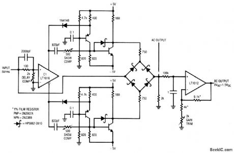
This circuit shows a synchronous-rectifier-based ac/dc converter which has high accuracy up to about 2.5 MHz. To calibrate, apply a 1- to 2-MHz 1-V pp sine wave and adjust the delay compensation so that bridge switching occurs when the sine crosses zero. Next, adjust both skew compensation pots for minimum aberrations in the ac output signal. Finally, adjust the gain trim for a dc output that corresponds to the ac input. (View)
View full Circuit Diagram | Comments | Reading(2262)
ADJUSTABLE_FINISH_CHARGE
Published:2009/6/29 Author:May
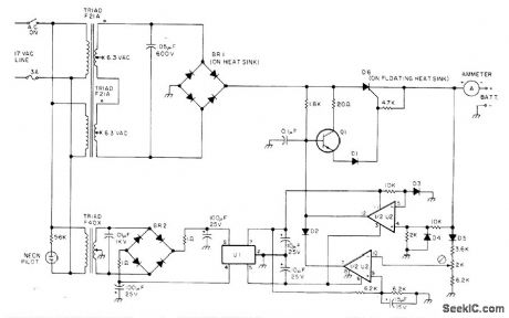
Uses National LM319D dual comparator U2 to sense end-of-charge battery voltage and provide protection against shorted or reversed charger leads. Final charging voltage for 12-V storage batteries is adjustable with 2K trimpot. Separate ±15 V supply using Raytheon RC4195NB regulator U1 is provided for U2. D1-D5 are 1N4002 or HEP-R0051. D6 is 2N682 or HEP-R1471. BR1 is Mo-torola MDA980-2 or HEP-B0876 12-A brldge. BR2 is Varp VE27 1-A bridge. Q1 is 2N3641 or HEP-S0015.-H. Olson, Battery Chargers Exposed, 73 Magazine, Nov. 1976, p 98-100 and 102-104. (View)
View full Circuit Diagram | Comments | Reading(866)
96_V_AT_20_mA
Published:2009/6/28 23:53:00 Author:May
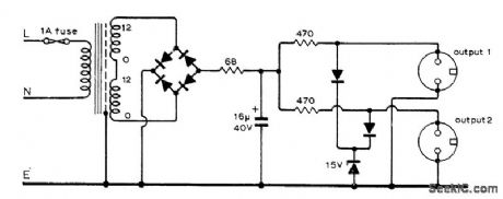
Developed to charge 200-mAh nickel-cadmium batteries for two transceivers simultaneously. Batteries will be fully charged in 14 hours, using correct 20-mA charging rate. Zone diode ensures that voltage cannot exceed safe value if battery is accidentally disconnected while under charge. Diode types are not critical.-D. A. Tong,A Pocket V.H.F. Transceiver, Wireless World, Aug, 1974 p 293-298. (View)
View full Circuit Diagram | Comments | Reading(669)
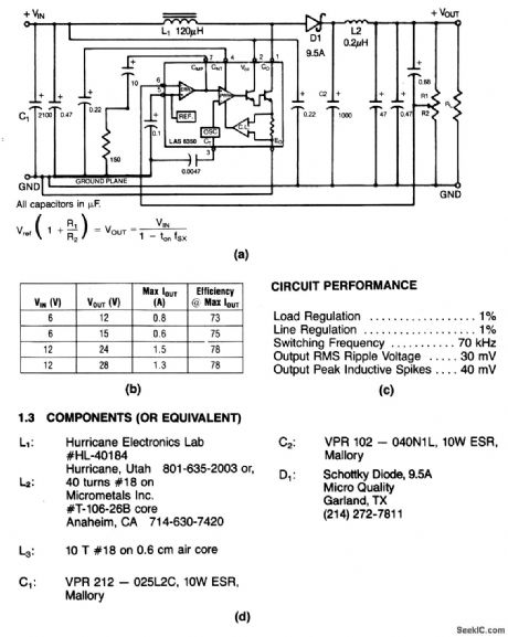
Adjustable_dc_dc_step-down_converter5_A
Published:2009/7/25 1:14:00 Author:Jessie
This circuit shows an LAS-6350/6450 used as a step-down converter with an adjustable output. (View)
View full Circuit Diagram | Comments | Reading(490)
Adjustable_dc_dc_step_up_converter_1_A
Published:2009/7/25 1:13:00 Author:Jessie
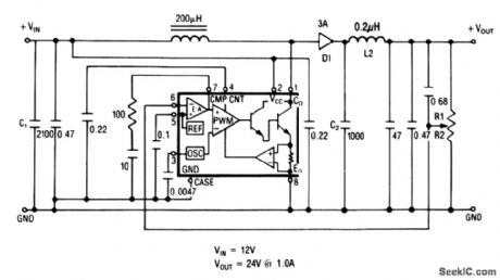
This circuit shows an LAS-6330/6430 used as a step-up converter with an adjustable output. (View)
View full Circuit Diagram | Comments | Reading(534)
Adjustable_dc_dc_step_down_converter_3_A
Published:2009/7/25 1:12:00 Author:Jessie
This circuit shows an LAS-6350/6450 used as a step-down converter with an adjustable output. (View)
View full Circuit Diagram | Comments | Reading(578)
Adjustable_dc_dc_step_up_converter_750_mnA
Published:2009/7/25 1:11:00 Author:Jessie
This circuit shows an LAS-6320P used as a step-up converter with anadjustable output. (View)
View full Circuit Diagram | Comments | Reading(570)
Adjustable_dc_dc_step_down_converer2A
Published:2009/7/25 1:10:00 Author:Jessie
This circuit shows an LAS-6320P used as a step-down converter with an adjustable output. (View)
View full Circuit Diagram | Comments | Reading(493)
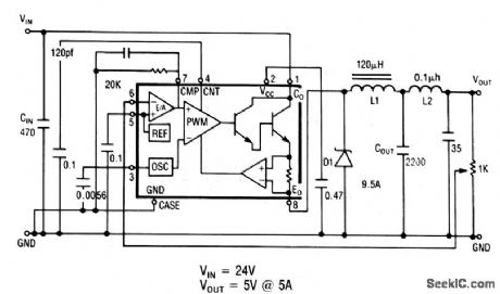
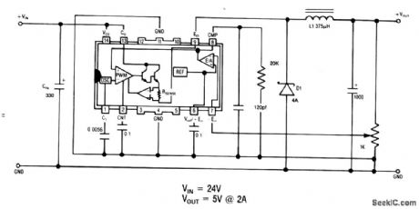
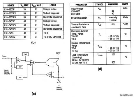
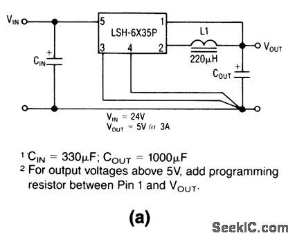
_8_A_dc_dc_step_down_converter
Published:2009/7/25 1:09:00 Author:Jessie
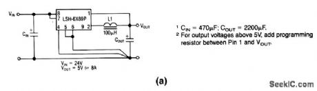
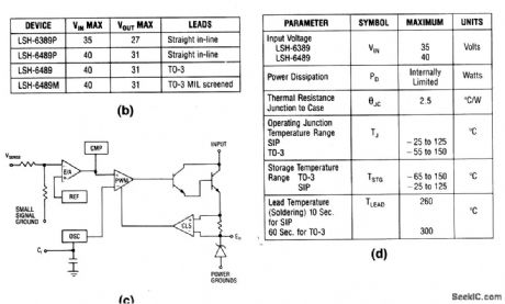
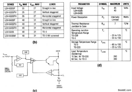
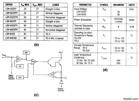
The LSH switching-regulator ICs contain most elements necessary for converter operation, as shown in Fig. 4-6C. Figure 4-6B shows the output voltage and characteristics for various part numbers. Figure 4-6D shows the absolute maximum ratings. Simply add a choke, catch diode, and two capacitors to the IC for a complete converter. (View)
View full Circuit Diagram | Comments | Reading(487)
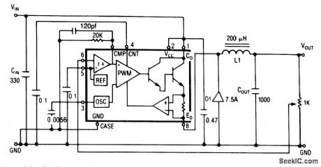
5_A_dc_dc_step_down_converter
Published:2009/7/25 1:07:00 Author:Jessie

The LSH switching-regulator ICs contain most elements necessary for converter operation, as shown in Fig. 4-5C. Figure 4-5B shows the output voltage and characteristics for various part numbers. Figure 4-5D shows the absolute maximum ratings. Simply add a choke, catch diode, and two capacitors to the IC for a complete converter. (View)
View full Circuit Diagram | Comments | Reading(641)
3_A_dc_dc_step_dowm_converter
Published:2009/7/25 1:04:00 Author:Jessie
The LSH switching-regulator ICs contain most elements necessary for converter operation, as shown in Fig. 4-4C. Figure 4-4B shows the output voltage and characteristics for various part numbers. Figure 4-4D shows the absolute maximum ratings. Simply add a choke, catch diode, and two capacitors to the IC for a complete converter. (View)
View full Circuit Diagram | Comments | Reading(546)
2_A_dc_dc_step_down_converter
Published:2009/7/25 1:00:00 Author:Jessie
The LSH switching-regulator ICs contain most elements necessary for converter operation, as shown in Fig. 4-3C. Figure 4-2B shows the output voltage and characteristics for various part numbers. Figure 4-3D shows the absolute maximum ratings. Simply add a choke, catch diode, and two capacitors to the IC for a complete converter. (View)
View full Circuit Diagram | Comments | Reading(439)
Dual_output_transformerless_converter
Published:2009/7/25 1:39:00 Author:Jessie
This circuit provides a dual output without transformers. Typical performance and component source information are shown in Figs. 4-30B and 4-30C, respectively. (View)
View full Circuit Diagram | Comments | Reading(620)
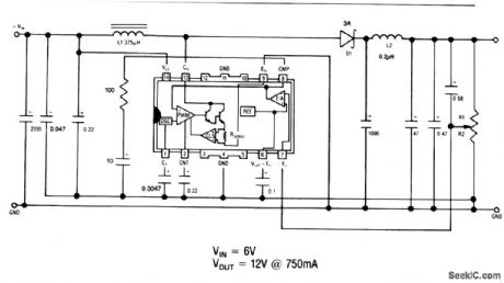
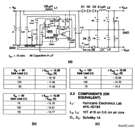
Step_up_converter_with_adjustable_output
Published:2009/7/25 1:38:00 Author:Jessie
This circuit provides an adjustable output at 1.5 A. Typical performance, circuit performance, and component sources are shown in Figs. 4-29B, 4-29C, and 4-29D, respectively. (View)
View full Circuit Diagram | Comments | Reading(448)
Triple_output_supply_5V_at_5A_±12V_at_125mA
Published:2009/7/25 1:36:00 Author:Jessie
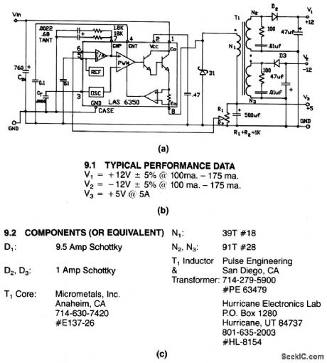
This circuit provides an adjustable +5-V and fixed ±12-V outputs,Figure 4-28B shows typical performance data,Figure 4-28C shows component source information. (View)
View full Circuit Diagram | Comments | Reading(616)
Dual_output_supply_±5_V
Published:2009/7/25 1:35:00 Author:Jessie
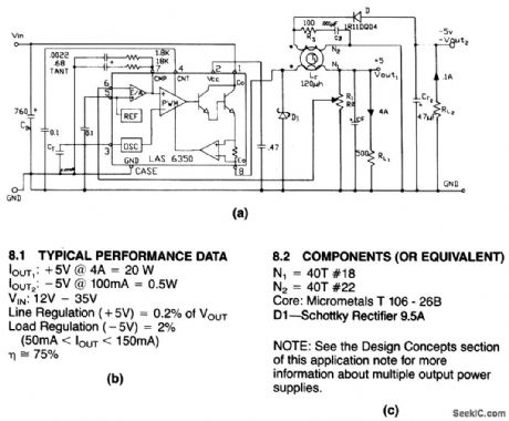
This circuit provides an adjustable +5-V and a fixed -5-V output. Figure 4-27B shows typical performance data.Figure 4-27C shows component source information. (View)
View full Circuit Diagram | Comments | Reading(573)
| Pages:163/291 At 20161162163164165166167168169170171172173174175176177178179180Under 20 |
Circuit Categories
power supply circuit
Amplifier Circuit
Basic Circuit
LED and Light Circuit
Sensor Circuit
Signal Processing
Electrical Equipment Circuit
Control Circuit
Remote Control Circuit
A/D-D/A Converter Circuit
Audio Circuit
Measuring and Test Circuit
Communication Circuit
Computer-Related Circuit
555 Circuit
Automotive Circuit
Repairing Circuit