
Index 167
PRECISION_HIGH_VOLTAGE_REGULATOR
Published:2009/6/28 22:07:00 Author:May
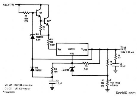
View full Circuit Diagram | Comments | Reading(1844)
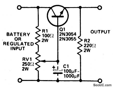
POWER_PACK_FOR_BATTERY_POWERED_CALCULATORS,RADIOS,OR_CASSETTE_PLAYERS
Published:2009/6/28 22:07:00 Author:May
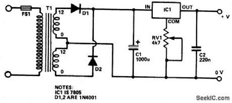
This circuit gives a regulated output of between 5 V and 15 Vdc, adjusted and set by a preset resistor. Current output up to about 350 mA. An integrated circuit regulates the output voltage and although this IC (the 7805) is normally used in a fixed-voltage (5 Vdc) supply it is for a variable output voltage. (View)
View full Circuit Diagram | Comments | Reading(593)
5_A_CONSTANT_VOLTAGE/CONSTANT_CURRENT_REGULATOR
Published:2009/6/28 22:04:00 Author:May
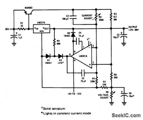
View full Circuit Diagram | Comments | Reading(1041)
12_V_TO_9,75_or_6_V_CONVERTER
Published:2009/6/28 22:02:00 Author:May
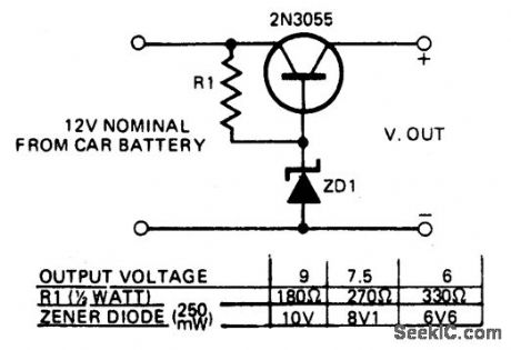
This circuit enables transistorized items such as radio, cassettes, and other electrical devices to be operated from a car's electrical supply. The table gives values for resistors and specified diode types for different voltage. Should more than one voltage be required a switching arrangement could be incorporated.For high currents, the transistor should be mounted on a heatsink. (View)
View full Circuit Diagram | Comments | Reading(425)
REGULATED_VOLTAGE_DIVIDER
Published:2009/6/28 22:01:00 Author:May
ICs requiring 3.6 or 6 volts can be run from a battery or fixed regulated supply of a higher voltage by using the circuit shown. The transistor should be mounted on a heatsink as considerable power will be dissipated by its collector.Additional filtering can be obtained by fitting a capacitor (C1) as shown. The capacitance is effectively multiplied by the gain of the transistor. A ripple of 200 mV (peak to peak) at the input can be reduced to 2 mV in this fashion. Maximum output current depends on the supply rating and transistor type (with heatsink) used. (View)
View full Circuit Diagram | Comments | Reading(1043)
RE_PROBE_FOR_VTVM
Published:2009/6/28 21:58:00 Author:May

This circuit combines a 555 timer with a 2N2222 transistor and an extemal potentiometer. The pot adjusts the output voltage to the desired value. To regulate the output voltage, the 2N2222 varies the control voltage of the 555 IC, increasing or decreasing the pulse repetition rate. A 1.2 K resistor is used as a collector load. The transistor base is driven from the extemal pot. If the output voltage becomes less negative, the control voltage moves closer to ground, causing the repetition rate of the 555 to increase, which, in turn, causes the 3 μF capacitor to charge more frequently. Output voltage for the circuit is 0 to 10 V, adjusted by the extemal pot. Output regulation is less than five percent for 0 to 10 mA and less than .05 percent for 0 to 0.2 mA. (View)
View full Circuit Diagram | Comments | Reading(597)
The 3-terminal stabilizer switch regulator power supply circuit
Published:2011/7/24 3:41:00 Author:Seven | Keyword: 3-terminal stabilizer, switch regulator

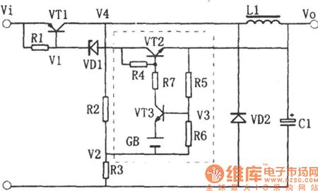
The switch regulator power supply circuit formed by the 3-terminal stabilizer can be understood by the equivalent circuit. As some reasons, the output voltage falls down slightly, the distributed voltage V3 on R5 and R6 is also falls down, after being amplified by VT3, IC3 decreases, i.e the current past R1 and VD1 is falling down, which leads to the drop of V1 and rise of IC1, V4 is rising up after being distributed by R2 and R3, V2 is rising up with it, accordingly, V3 falls```
(View)
View full Circuit Diagram | Comments | Reading(493)
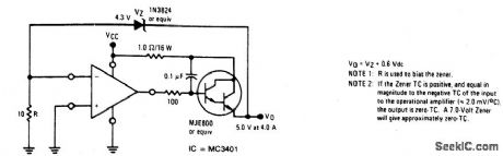
ADJUSTABLE_OUTPUT_REGULATOR
Published:2009/6/28 21:57:00 Author:May
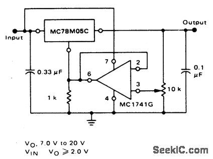
The addition of an operational amplifier allows adjustment to higher or intermediate values while retaining regulation characteristics; The minimum voltage obtainable with this arrangement is 2.0 volts greater than the regulator voltage. (View)
View full Circuit Diagram | Comments | Reading(649)
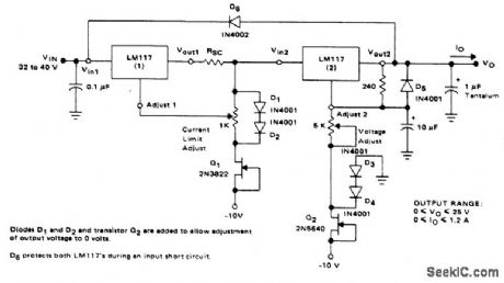
POWER_SUPPLY_WITH_ADJUSTABLE_CURRENT_LIMIT_AND_OUTPUT_VOLTAGE
Published:2009/6/28 21:56:00 Author:May
View full Circuit Diagram | Comments | Reading(1295)
DUAL_OUTPUT_BENCH_POWER_SUPPLY
Published:2009/6/28 21:55:00 Author:May
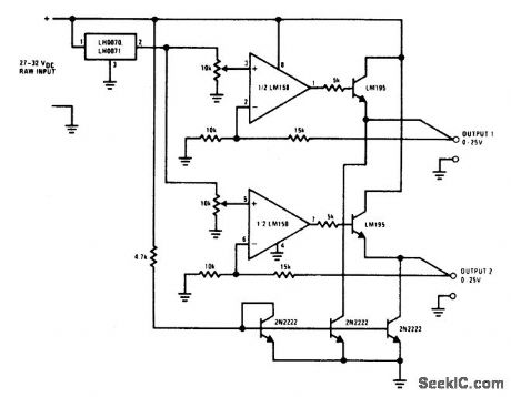
View full Circuit Diagram | Comments | Reading(570)
100_V/025_A_SWITCH_MODE_CONVERTER
Published:2009/6/28 21:53:00 Author:May
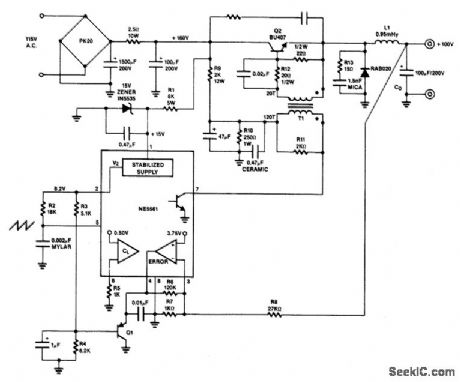
View full Circuit Diagram | Comments | Reading(554)
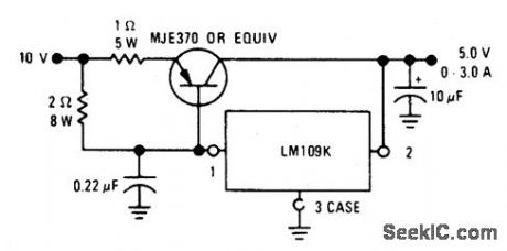
HIGH_STABILITY_1_A_REGULATOR
Published:2009/6/28 21:52:00 Author:May
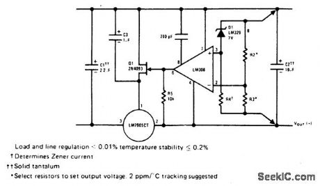
View full Circuit Diagram | Comments | Reading(434)
LOW_VOLTAGE_REGULATORS_WITH
Published:2009/6/28 21:51:00 Author:May
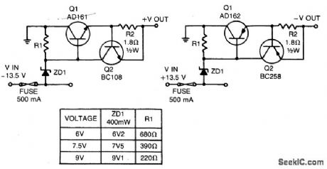
These short-circuit protected regulators give 6, 7.5, and 9 V from an automobile battery supply of 13.5 V nominal; however, they will function just as well if connected to a smoothed dc output from a transformer/rectifier circuit.Two types are shown for both positive and negative ground systems. The power transistors can be mounted on the heatsink without a mica insulating spacer thus allowing for greater cooling efficiency. Both circuits are protected against overload or short-circuits. The current cannot exceed 330 mA. Under normal operating conditions the voltage across R2 does not rise above the 500 mV necessary to turn Q2 on and the circuit behaves as if there was only Q1 present. If excessive current is drawn, Q2 turns on and cuts off Q1, protecting the regulating transistor. The table gives the values of R1 for different zener voltages. (View)
View full Circuit Diagram | Comments | Reading(928)
VOLTAGE_REGULATOR
Published:2009/6/28 21:49:00 Author:May
View full Circuit Diagram | Comments | Reading(0)
10_V/025_A_SWITCH_MODE_CONVERTER
Published:2009/6/28 21:48:00 Author:May
View full Circuit Diagram | Comments | Reading(565)
50_V/30_A_REGULATOR
Published:2009/6/28 21:46:00 Author:May
View full Circuit Diagram | Comments | Reading(520)
50_V/10_A_REGULATOR
Published:2009/6/28 21:45:00 Author:May
View full Circuit Diagram | Comments | Reading(501)
MOBILE_VOLTAGE_REGULATOR
Published:2009/6/28 21:34:00 Author:May
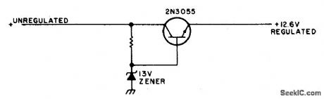
This simple mobile voltage regulator circuit may save your two meter or CB transceiver if the voltage regulator fails. The 2N3055 should be heat sinked if current drawn by the rig is in excess of 2 A on transmit. This circuit will do little under normal operating conditions, but could save expensive equipment if the vehicle's electrical system loses regulation. (View)
View full Circuit Diagram | Comments | Reading(1188)
DUAL_POLARITY_POWER_SUPPLY
Published:2009/6/28 21:30:00 Author:May
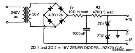
This simple circuit gives a positive and negative supply from a single transformer winding and one full-wave bridge. Two zener diodes in series provide the voltage division and their centerpoint is grounded. (The filter capacitor must not be grounded via its case). (View)
View full Circuit Diagram | Comments | Reading(2007)
TRANSISTOR_INCREASES_ZENER_RATING
Published:2009/6/28 21:28:00 Author:May
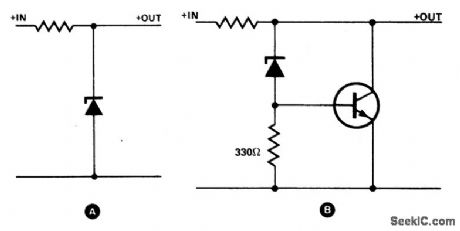
The simple zener shunt in A may not handle sufficient current if the zener available is of low wattage. A power transistor will do most of the work for the zener as shown in B. Once the zener starts conducting, a bias voltage develops across the resistor (330 Ω to 1K), turning on the transistor. The output voltage is 0.7 V greater than the zener voltage. (View)
View full Circuit Diagram | Comments | Reading(536)
| Pages:167/291 At 20161162163164165166167168169170171172173174175176177178179180Under 20 |
Circuit Categories
power supply circuit
Amplifier Circuit
Basic Circuit
LED and Light Circuit
Sensor Circuit
Signal Processing
Electrical Equipment Circuit
Control Circuit
Remote Control Circuit
A/D-D/A Converter Circuit
Audio Circuit
Measuring and Test Circuit
Communication Circuit
Computer-Related Circuit
555 Circuit
Automotive Circuit
Repairing Circuit