
Index 170
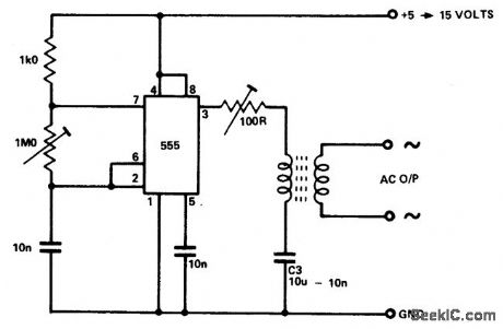
NEON_LAMP_DRIVER_FOR_5_TO_15_V_SUPPLIES
Published:2009/6/26 3:51:00 Author:Jessie
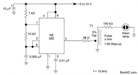
This neon-lamp driver based on the 555 T1 can be wound on an old TV flyback transformer core. (View)
View full Circuit Diagram | Comments | Reading(3489)
CURRENT_LIMITING_REGULATOR
Published:2009/6/26 3:49:00 Author:Jessie
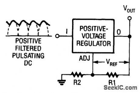
Floating adjustable regulators can be used as current Iimiters. Resistor R1 programs the current flowing through R2. (View)
View full Circuit Diagram | Comments | Reading(874)
MULTIVOLTAGE_POWER_SUPPLY
Published:2009/6/26 3:49:00 Author:Jessie
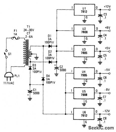
This dual-polarity, multivoltage power supply can be built for a very small investment. The circuit is built around 78XX and 79XX series 1-A voltage regulators, four 3-A diodes, a 24-30-V 2-6-A transformer, and eight filter capacitors. (View)
View full Circuit Diagram | Comments | Reading(1902)
INVERTING_POWER_SUPPLY
Published:2009/6/26 3:43:00 Author:Jessie
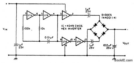
This circuit will provide a negative dc voltage that is approximately equal to the positive input voltage at no load and about 3 V less at 10 mA load. VIN is from +5 to +15 Vdc, Do not exceed 15 V or U1 might be damaged. (View)
View full Circuit Diagram | Comments | Reading(623)
SIMPLE_NEGATIVE_SUPPLY_FOR_LOW_CURRENT_APPLICATIONS
Published:2009/6/26 3:41:00 Author:Jessie
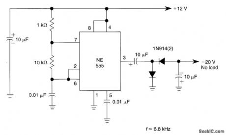
This dc negative-voltage generator based on the 555 produces a negative output voltage equal to approximately 2x the dc supply voltage. (View)
View full Circuit Diagram | Comments | Reading(1054)
1_kHz_MODULATOR_FOR_VHF_SOURCE
Published:2009/6/26 3:02:00 Author:Jessie
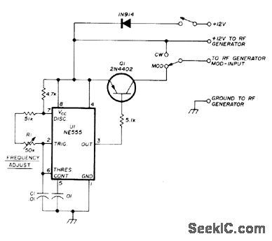
Used with 144-MHz signal generator driving VSWR bridge, for measuring and matching VHF antennas. R1 adjusts frequency of NE555 timer used in place of customary MVBR. Series-pass transistor increases output of MVBR about 2 dB.-J. Reisert, Matching Techniques for VHF/UHF Antennas, Ham Fladio, July 1976, p 50-56. (View)
View full Circuit Diagram | Comments | Reading(1026)
±10_V_FULL_SCALE_BIPOLAR_DAC
Published:2009/6/26 2:37:00 Author:Jessie
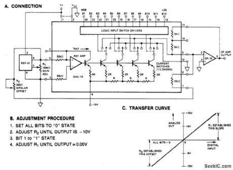
View full Circuit Diagram | Comments | Reading(1186)
50_MHz_POWER
Published:2009/6/25 21:49:00 Author:May
Developed for use with 50 MHz microtransistor crystal oscillator,using additional GE microtransistor for boosting RF output to about 75 mW,Article covers construction with microcomponents and gives other microtransistor circuits for low-power amateur tadiouse and possible bugging applications,-B.Hoisington、Introduction to″Microtransistors,″73 Magazit, Oct.1974,p 24-30. (View)
View full Circuit Diagram | Comments | Reading(1245)
SOUND_MODULATED_LIGHT_SOURCE
Published:2009/6/25 21:16:00 Author:May
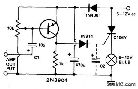
This circuit modulates a light beam with voice or music from the output of an amplifier. If the 10 K pot is adjusted to slightly less than the Vbe of the transistor, the circuit forms a peak detector. This drives the gate of the SCR, lighting the bulb whose brightness will vary as the sound level varies. C2 may be removed for a faster response. (View)
View full Circuit Diagram | Comments | Reading(702)
CAPACITANCE_MULTIPLIER
Published:2009/6/25 21:09:00 Author:Jessie
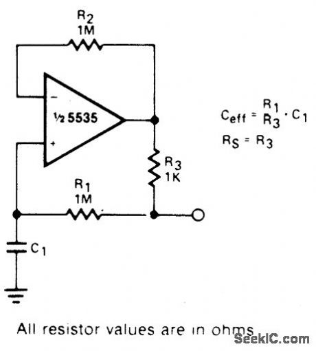
This circuit can be used to simulate large capacitances using small value components. With the values shown and C = 10 μF, an effective capacitance of 10,000 μF was obtained. The Q available is limited by the effective series resistance. So R1 should be as large as practical (View)
View full Circuit Diagram | Comments | Reading(0)
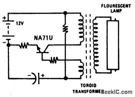
MINI_POWER_INVERTER_AS_HIGH_VOLTAGELOW_CURRENT_SOURCE
Published:2009/6/25 4:34:00 Author:May
Circuit Notes
The circuit is capable of providing power for portable Geiger counters, dosimeter char-gers, higlt resistance meters, etc. The 555 timer IC is used in its multivibrator mode, the frequency adjusted to optimize the transformer characteristics. When the output of the IC is high, current flows through the limiting resis-tor, the primary coil to charge C3. When the output is low, the current is reversed. With a suitable choice of frequency and C3, a good symmetric output is sustained. (View)
View full Circuit Diagram | Comments | Reading(1026)
NEGATIVE_TO_POSITIVE_SUPPLY_LOGIC_LEVEL_SHIFTER
Published:2009/6/25 3:13:00 Author:May
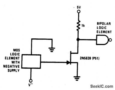
This simple circuit provides for level shifting from any logic function (such as MOS) operating from minus to ground supply to any logic level (such as TTL) operating from a plus to ground supply. The 2N5639 provides a low rdc (ON) and fast switching times. (View)
View full Circuit Diagram | Comments | Reading(772)
CURRENT_SOURCE
Published:2009/6/25 3:52:00 Author:May
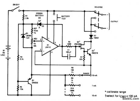
Circuit Notes
This precision current source has 10 μA to 10 mA ranges with output compliance or 30V to -5V. Output current is fully adjustable oneach range with a calibrated, ten-turn potentiometer. Error light indicates saturation. (View)
View full Circuit Diagram | Comments | Reading(2512)
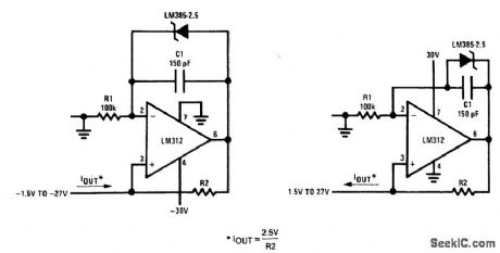
PRECISION_1_μA_to_1_mA_CURRENT_SOURCES
Published:2009/6/25 4:06:00 Author:May
View full Circuit Diagram | Comments | Reading(570)
PRECISION_CURRENT_SOURCE
Published:2009/6/25 3:53:00 Author:May

Circuit Notes
The 2N5457 and PN2222 bipolar serve as voltage isolation devices between the output and the current sensing resistor, R1. The LM101 provides a large amount of loop gain to assure that the circuit acts as a current source. For small values of current (<1 mA), the PN2222 and 10K resistor may be eliminated with the outpuf appearing at the source of the 2N5457. (View)
View full Circuit Diagram | Comments | Reading(0)
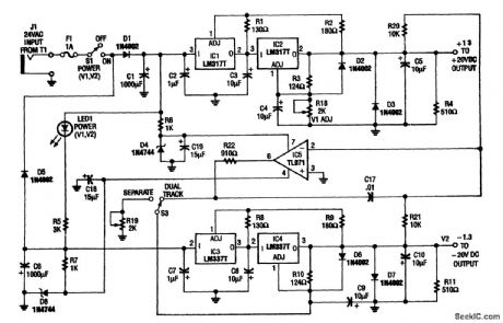
SINGLE_LTC_POWER_SUPPLY
Published:2009/6/25 2:56:00 Author:May
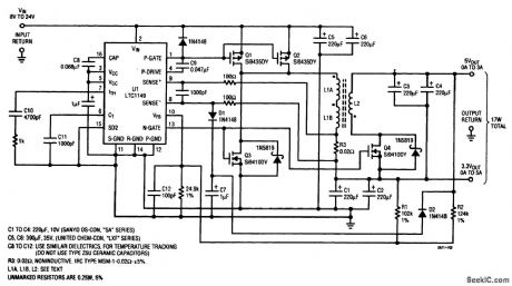
One LTC 1149 synchronous switching regulator can deliver both 3.3- and 5-V outputs. The design's simplicity, low cost, and high efficiency make it a strong contender for portable, battery-powered applications. The circuit described accepts input voltages from 8 to 24 V, to power any combination of 3.3-V and 5-V loads totalling 17 W or less. For input voltages in the 8-V to 16-V range, the LTC1148 may be used, reducing both quiescent current and cost. (View)
View full Circuit Diagram | Comments | Reading(542)
_5_V__36_V_FROM_4_AA_CELLS
Published:2009/6/25 2:28:00 Author:Jessie
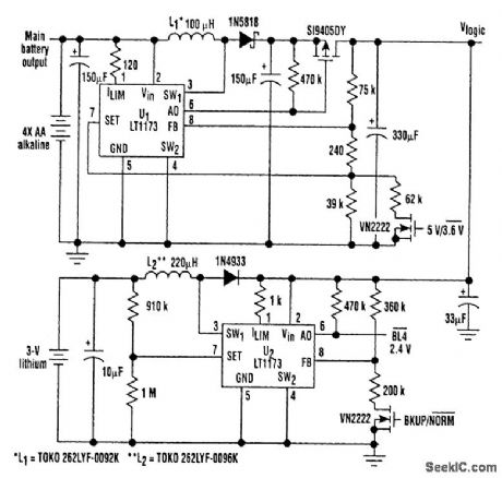
With this unique logic-power-converter design (see the figure), a switchable 3.6 or 5 V at 200 mA can be attained by using four AA cells. The supply incorporates a MOSFET switch that can switch to a lithium backup battery, providing a 3.4-V output when the main battery is dead or removed. The supply consumes only 380 pA under no-load conditions.
The circuit operates in a somewhat novel mode as a step-up/step-down converter. When the cells are fresh (from about 6 V to about 5.2 V), the LT1173's gain block drives the p-channel MOSFET, which turns the circuit into a linear voltage regulator. This might seem inefficient, but the batteries are quick to drop from 6 V to 5 V. With a 5-V input, the efficiency (for the 3.6-V output) is 3.6/5 or 72%, which is reasonable. As the battery-pack drops in voltage, efficiency increases, reaching greater than 90% with a 4.2-V input.
At a point below a 4-V input, the circuit switches to step-up mode. This mode squeezes the bat-teries for all of their available energy. In this case, efficiency runs between 83% at approximately a 4-V input to 73% at a 2.5-V input.
The supply can deliver 200 mA over its entire operational range. In its linear mode of operation, the supply has no current spikes that, because of the fairly high internal resistance of the alkaline cells, can reduce battery life. The topology delivers over 9.3 hours of 3.6-V 200-mA output power, compared to just 7 hours using the traditional flyback topology that is used in other designs. (View)
View full Circuit Diagram | Comments | Reading(689)
UNIVERSAL_LABORATORY_POWER_SUPPLY
Published:2009/6/25 2:21:00 Author:May
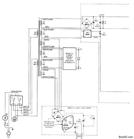
The value of the design lies in the use of IC1,an LM317HVK adjustable serles-pass voltage regulator,for broad-range performance remainder supplies voltage-setting and current limiting functions The input to IC1 comes from the output of BR1,which is filtered by C1 and C2 to about +60Vdc,and the input for current-sense comparator IC2 comes from BR2,which also acts as a negative bias supply for regulation down to ground. The output voltage is determined by∶( VOUT - 1.25 + 1.3 ) /( R15 + R16 ) = 1.25 / R8.Thus,the maximum value from each variable supply board is∶VOUT = ( 1.25 / R8 ) × ( R15 + R16 ) = 50.18 Vdc (View)
View full Circuit Diagram | Comments | Reading(2045)
BATTERY_LANTERN_CIRCUIT_
Published:2009/6/25 2:15:00 Author:May
View full Circuit Diagram | Comments | Reading(868)
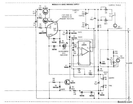
TRACKING_DOUBLE_OUTPUT_BIPOLAR_SUPPLY
Published:2009/6/25 2:05:00 Author:May
This circuit is useful for a bench supply in the lab. Separate or tracking operation is possible. The regulators should be properly heatsinked. T1 is a 24-Vac wall transformer of suitable current capacity. (View)
View full Circuit Diagram | Comments | Reading(711)
| Pages:170/291 At 20161162163164165166167168169170171172173174175176177178179180Under 20 |
Circuit Categories
power supply circuit
Amplifier Circuit
Basic Circuit
LED and Light Circuit
Sensor Circuit
Signal Processing
Electrical Equipment Circuit
Control Circuit
Remote Control Circuit
A/D-D/A Converter Circuit
Audio Circuit
Measuring and Test Circuit
Communication Circuit
Computer-Related Circuit
555 Circuit
Automotive Circuit
Repairing Circuit