
Index 172
BATTERY_CHARGER
Published:2009/6/24 22:11:00 Author:May
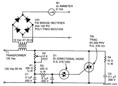
A diac is used in the gate circuit to provide a threshold level for firing the triac. C3 and R4 provide a transient suppression network. RI, R2, R3, C1, and C2 provide a phase-shift network for the signal being applied to the gate. R1 is selected to limit the maximum charging cur-rent at full rotation of R2. (View)
View full Circuit Diagram | Comments | Reading(0)
SYNC_TIP_dc_RESTORER
Published:2009/6/24 3:26:00 Author:Jessie
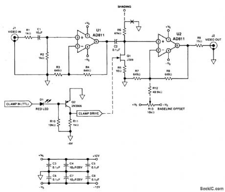
The dc restorer shown supplies a video signal with sync tips clamped to a baseline level. Clamp drive signal is supplied from elsewhere, usually a sync generator or a sync separator. (View)
View full Circuit Diagram | Comments | Reading(3070)
FLYBACK_POWER_SUPPLY_FOR_RADON_MONITOR
Published:2009/6/24 3:23:00 Author:Jessie
This blocking-oscillator flyback circuit is an alternative for charging the ionization chamber capacitor. (View)
View full Circuit Diagram | Comments | Reading(2255)
VARIABLE_VOLTAGE_REGULATOR_WITH_WIDE_RANGE_CURRENT_LIMITING
Published:2009/6/24 2:56:00 Author:May
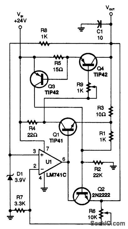

In this circuit,R9 acts as a control to set current limiting。If R9=0,limiting occurs at 47 mA.Input is 24 V, output isdepending on the setting of R6. (View)
View full Circuit Diagram | Comments | Reading(781)
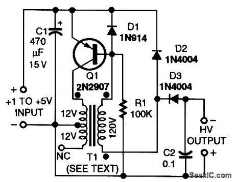
-100_Vdc_SUPPLY
Published:2009/6/24 1:42:00 Author:May
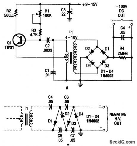
The combination Hartley oscillator/step-up transformer shown in A can generate significant negative high-voltage-especially if the voltage output of the transformer is multiplied by the circuit in Fig.69-5B. T1 is a small low-voltage filament transformer of around 4- to 10-Vac output, 120-V primary. (View)
View full Circuit Diagram | Comments | Reading(862)
_GENERAL_PURPOSE_0_TO_30_V_POWER_SUPPLY__
Published:2009/6/24 2:56:00 Author:May
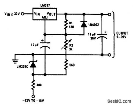
View full Circuit Diagram | Comments | Reading(586)
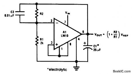
ADJUSTABLE_BIAS_REGULATOR
Published:2009/6/24 2:59:00 Author:Jessie
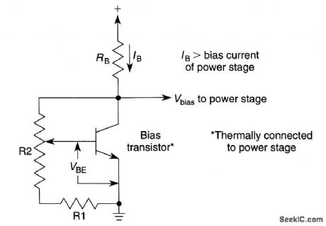
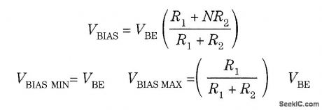
If the wiper of R2 is set at N% rotation,the bias voltage Will be∶This method derives a bias voltage that tracks VBE of this bias transistor. If the bias transistor is thermally linked to the power stage, tracking over a wide temperature range will result. (View)
View full Circuit Diagram | Comments | Reading(1075)
ADJUSTABLE_POSITIVE_REGULATOR
Published:2009/6/24 2:57:00 Author:Jessie
View full Circuit Diagram | Comments | Reading(883)
ADJUSTABLE_POWER_SUPPLY
Published:2009/6/24 2:53:00 Author:Jessie
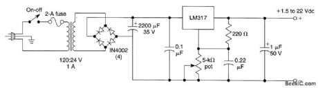
Using an LM317, this supply delivers 1.25 to 22 Vdc for various purposes. The LM317 should be heatsinked. This supply will deliver 600-mA output current. (View)
View full Circuit Diagram | Comments | Reading(979)
TRANSCEIVER_POWER_SUPPLY_FOR_VARIABLE_LAB_SOURCE
Published:2009/6/24 2:51:00 Author:Jessie

A variable voltage regulator provides 1 to 11 Vdc for lab bench work,using an existing 13.8-V transceiver supply. (View)
View full Circuit Diagram | Comments | Reading(3639)
ADJUSTABLE_0_TO_5_V_SUPPLY
Published:2009/6/24 2:50:00 Author:Jessie
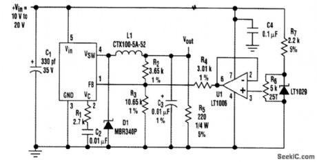
Although linear-regulator ICs are frequently used In variable p。wer-supply applications,they might not always be the best choice,At low output voltages,power losses in these regulators cancause headaches for designers For example,if an output current of 1.25 A is required at 1.25 V from an input of 8 V.a regulator (such as the LT317)dissipates more than 10 W.The figure depicts a dc-dc converter that functionally replaces a linear regulator in the just clescribed application. The converter not only-eliminates the problem of power loss,but it can be adjusted for output voltages (as low as 25 mV)while delivering an output current of 1.5 A.The circuit uses a basic positive-buck topology with one exception,A control voltage is applied through R4 to the feedback summing node at pin of the LT1076 regulator IC,making it possible to adjust the output from0 V to approximately 6 V. This range encompasses the 3.3-V and 5-V logic supplyvoltages for portable and desktop equipment,as well as battery-pack combinations of one to four cells.As R4is driven from0 to 5 V by the buffer (U1),more or less current is required from R2 to satisfy the loop’s desire to hold the feedback summing point at 2.37V. This forces the converter’s out-put to swlng over the range of0 to 6 V.The LT1076 is capable of 1.75-A guaranteed output current In this application,and 2 A is typical.If more current is required,the LT1074 can be substituted for the LT1076. (View)
View full Circuit Diagram | Comments | Reading(1529)
±15_V_POWER_SUPPLY
Published:2009/6/24 2:39:00 Author:May
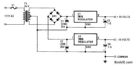
A simple bridge rectifier feeds two IC regulators. This circuit should be useful for op-amp circuitry. (View)
View full Circuit Diagram | Comments | Reading(2344)
GENERAL_PURPOSE_POWER_SUPPLY_FOR_AUTOMOTIVE_PROJECTS
Published:2009/6/24 2:38:00 Author:May
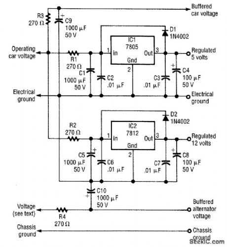
This supply produces 12 V and 5 V for a variety of automotive projects. F4 is connected directly to the alternator field winding (usable only if your car has a separate regulator). (View)
View full Circuit Diagram | Comments | Reading(527)
CCFL_SUPPLY_WITH_VARIABLE_CONTRAST
Published:2009/6/24 2:28:00 Author:May
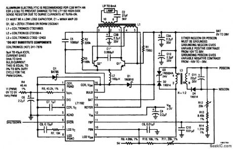
The figure is a complete floating CCFL circuit with variable negative/variable positive-contrast voltage capability, based on the LT1182. Lamp current is programmable from 0 mA to 6 mA using a 0- to 5-V 1-kHz PWM signal at 0% to 90% duty cycle. LCD contrast output voltage polarity is determined by which side of the transformer secondary (either POSCON or NEGCON) the output connector grounds. In either case, LCD contrast output voltage is variable from an absolute value of 10 V to 30 V. The input supply voltage range is 8 V to 28 V. The CCFL converter is optimized for photometric output per watt of input power. CCFL electrical efficiency up to 90% is possible and requires strict attention to detail. LCD contrast efficiency is 82% at full power. (View)
View full Circuit Diagram | Comments | Reading(1461)
Power Supply Circuit of Modem User Interface Circuit
Published:2011/7/22 22:02:00 Author:Michel | Keyword: Modem User Interface, Power Supply Circuit
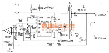
The above picture is power supply circuit of modem user interface circuit.The circuit consists of single power switch and control integrated circuit etc.It provides the multiple output voltage, power switch can also use N channels MOSFET of low voltage.The input power comes from different output power of AC adapter or the regualted power of parts of the system.UCC3813-5 is power control device and it controls output voltage via contolling VT1 dutyfactor and it provides reference voltage for inverse amplifier of error signal.UCC3813-5 can realize current control mode and the voltage control method.The biggest characteristic of this circuitis to use a control circuit and a MOSFET to provide two telephones voltage. (View)
View full Circuit Diagram | Comments | Reading(921)
ACTIVATE_BACK_UP_POWER_SUPPLY
Published:2009/6/24 2:24:00 Author:May


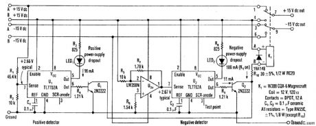
A circuit,which can be built around two TI TL7702 chips, monitors a 15-V power supply and activates a relay to turn on a back-up supply if the voltage drops below±14.1 V. With the back-up in place, the malfunctioning supply can be replaced without any down time. The TL7702 power-supply voltage supervisor chips are intended for use as reset controllers in microprocessor systems, but they work well in their modified form for this application.One chip detects the positive supply (U1),and the other is used for the negative (U2). A pair of output-relay drive transistors,Q1 and Q2 form a wired OR circuit so that relay K1 is activated by the positive or negative voltalge detector that switches U1 or U2 on.The supervisor chips have a direct connection to the input comparator so that the trigger level is set by a resistor-divider network (R1 and R2) at the sense-input pin.These chip also have an internal, stable, reference-voltage source set at +2.53V,typical.The positive-sensed voltage drops enough to activate the comparator, its output goes low,switches the internal gate,and triggers the siliconcontrolled rectifier (SCR).The output comparator then forces the two output transistors (pin 6) turn on the relay driver,Q1.The negative detector is preceded by halt of the dual op amp LM358N (U3a)-an inverting amplifier with a gain of-0.178.R5 connects to the -15 Vdc being sended. The output of U3a is usually set at 2.67 V, higher than the +2.53-V referenCe voltage. Therefore, no switching occurs. If the -15-Vdc voltage decreases, U2 switihes Q2 and activates K1 in the same manner as described for the U1-Q1 positive detector. R3, R4, and R8 through R10 serve as current-ltmtttng reststois. (View)
View full Circuit Diagram | Comments | Reading(942)
HIGH_EFFICIENCY_TRIPLE_OUTPUT_SUPPLY_FOR_NOTEBOOK_COMPUTERS
Published:2009/6/24 2:37:00 Author:Jessie
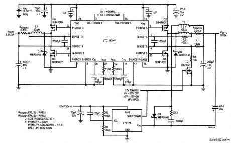
The circuit is conftgured to provide output voltages of 3.3 V, 5 V, and 12 V. The current capability of both the 3.3-V and 5-V outputs is 2 A (2.5 A peak). The logic controlled 12-V output can provide 150 mA (200 mA peak), which is ideal for flash memory applications. The operating efficiency shown in the ftgure exceeds 90% for both the 3.3-V and 5-V sections.The 3.3-V section for the circuit in the figure is comprised of the main switch Q4, synchronous switch Q5, inductor L1, and current shunt RSENSE. Current-sense resistor RSENSE monitors the inductor current and is used to set the output current accord-ing to the formula OUT = 100 mV/RSENSE. Advantages of current control include excellent line and load transient rejection, inher-ent short-circuit protection, and controlled start-up currents. Peak inductor currents for L1 and T1 for the circuit in the figure are limited to 150 mV/RSENSE or 3.0 A and 3.75 A, respectively. (View)
View full Circuit Diagram | Comments | Reading(538)
SIMPLE_CODE_PRACTICE_OSCILLATOR
Published:2009/6/24 2:33:00 Author:Jessie
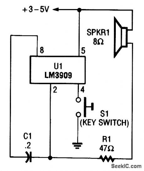
With only a minor circuit change, the basic LM3909 oscillator configuration can be turned into a code-practice oscillator. (View)
View full Circuit Diagram | Comments | Reading(1440)
STABLE_VFO_POWER_SUPPLY
Published:2009/6/24 2:31:00 Author:Jessie
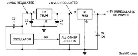
A dc power-distribution system for a stable oscillator should use a separate voltage regulator just for the oscillator circuit. (View)
View full Circuit Diagram | Comments | Reading(522)
dc_POWER_SOURCE_FOR_EXPERIMENTS
Published:2009/6/24 2:30:00 Author:Jessie
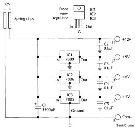
This supply uses IC regulators to supply +5, +6, +9, and +12 volts regulated from a nominal 12-V supply. (View)
View full Circuit Diagram | Comments | Reading(1907)
| Pages:172/291 At 20161162163164165166167168169170171172173174175176177178179180Under 20 |
Circuit Categories
power supply circuit
Amplifier Circuit
Basic Circuit
LED and Light Circuit
Sensor Circuit
Signal Processing
Electrical Equipment Circuit
Control Circuit
Remote Control Circuit
A/D-D/A Converter Circuit
Audio Circuit
Measuring and Test Circuit
Communication Circuit
Computer-Related Circuit
555 Circuit
Automotive Circuit
Repairing Circuit