
Index 180
BATTERY_SAVER_CIRCUIT
Published:2009/6/17 1:48:00 Author:May
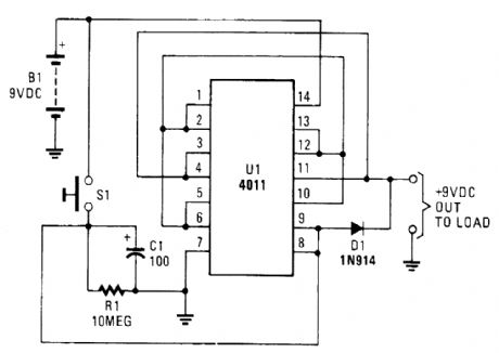
This battery saver circuit can automatically turn off a small piece of test equipment after a desired period of time, allowing you to leave your shop worry free.This circuit uses a CD4011 IC to act as a simple timer. One section acts as an RC discharge timer (pin 7). This causes its output to go low, holding the three other outputs high acting as a 9-V source.After C1/R1 discharges approximately 10 minutes, the output drops to zero. S1 resets the circuit. (View)
View full Circuit Diagram | Comments | Reading(2988)
LASER_POWER_SUPPLY
Published:2009/6/16 23:39:00 Author:May
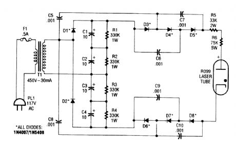
This supply generates an initial high voltage for ignition purposes. After ignition, the supply gen-erates about 1300 to 1500 V. If a higher ignition voltage (than the 6000 V supplied) is necessary, more multiplier stages can be added to D5 and D8. (View)
View full Circuit Diagram | Comments | Reading(1766)
HIGH_VOLTAGE_POWER_SUPPLY
Published:2009/6/16 23:37:00 Author:May
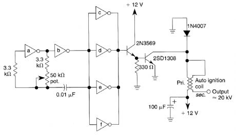
The high-voltage power supply is a CMOS-based oscillator that pulses a high-voltage ignition transformer. The transformer output is around 20 kV. (View)
View full Circuit Diagram | Comments | Reading(1399)
HANDHELD_LASER
Published:2009/6/16 23:35:00 Author:May
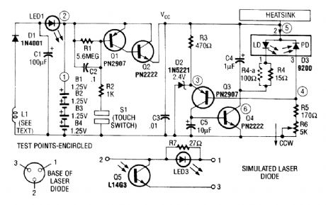
A laser diode TOLD9200 (Toshiba) is used as a source of laser light. Q3, Q2, and S1 form a touch switch to control the laser. L1 is an RF pickup coil to pick up energy from an RF-type battery charger.It is 10 tums of #18 wire on a 1/2 diameter. (View)
View full Circuit Diagram | Comments | Reading(1375)
LASER_POWER_SUPPLY_AND_STARTING_CIRCUIT
Published:2009/6/16 23:34:00 Author:May

This circuit delivers 10 kV peak, then limits current to 7.5 mA @ 2 kV. The resistors shown provide ballasting. The starting circuit cannot maintain the 10 kV under load and appears as a seriespass circuit with little drop in voltage. (View)
View full Circuit Diagram | Comments | Reading(577)
EFFICIENT_LASER_SUPPLY
Published:2009/6/16 23:32:00 Author:May

Driving Helium-Neon Lasers can be simplified considerably using this power-supply configura-tion. When power is applied, the laser doesn't conduct and the voltage across the 190-Ω resistor is zero. However, a resonant circuit and a voltage tripler then produces over 10 kV to turn on the laser. (View)
View full Circuit Diagram | Comments | Reading(1319)
INTELLIGENT_BATTERY_CHARGING_CIRCUIT
Published:2009/6/16 3:35:00 Author:May
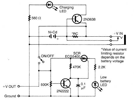
Intended for a Nicad application this charging circuit can be used with a wide range of batteries. A low-battery detector is intended. The trip voltage is set via the 500-kΩ pot. Select R, for the battery you intend to use. (View)
View full Circuit Diagram | Comments | Reading(1031)
SOLAR_POWERED_BATERY_CHARGER
Published:2009/6/16 3:30:00 Author:May
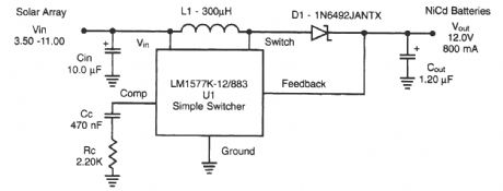
A National Semiconductor LM1577 IC is used in a step-up regulator to charge Nicad batteries from a solar panel. (View)
View full Circuit Diagram | Comments | Reading(2033)
BATTER_CHARGER
Published:2009/6/16 3:13:00 Author:May
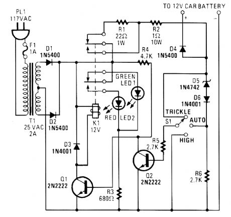
The circuit is capable of supplying either a trickle (50 mA) or high-current (1-A) charge. You can select either charging dtethod or an automatic mode that will first trickle charge a battery if it is particularly low before switching to high-current charging.If the battery's voltage is low, Zener-diode D5 will not conduct sufficient current to produce a voltage drop across R6 to turn Q2 on. With Q2 off, R4 pulls the base of Q1 high, turning it on. That activates K1. With K1 active, the only thing between the battery and the power supply is R2 and D4 (which prevents current from flowing through the circuit from the battery).Once the battery charges a bit, the current through D5 increases, causing a voltage drop across R6 that is of sufficient magnitude to turn on Q2. Transistor Q2, in turn, grounds the base of Q1, keeping it off. With Q1 off, K1 remains in its normally closed state. That places R1 in series with the battery, thereby reducing the current to a trickle. (View)
View full Circuit Diagram | Comments | Reading(1597)
RF_TYPE_BATTERY_CJARGER
Published:2009/6/16 3:08:00 Author:May
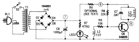
This type of charger couples RF from L2 to an external pickup coil The pickup coil connects to a rectifier and batteryto be charged This idea is handy because no wire or contacts are required L2 is 10T #24 wire and L3 is 10T #30 wire. Both cois are mounted on a 1''×1/4'' ferrite rod. (View)
View full Circuit Diagram | Comments | Reading(943)
LEAD_ACID_TRICKLE_CHARGER
Published:2009/6/16 3:08:00 Author:May
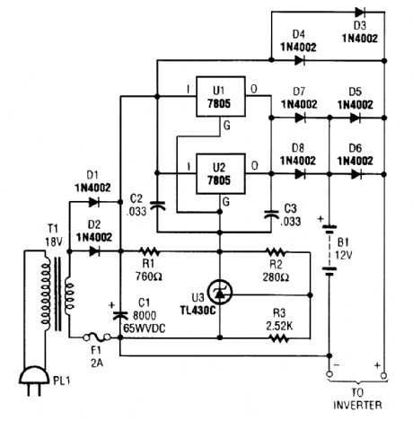
The charger can be used as a stand-alone charger or for emergency lighting and burglar alarm systems using lead-acid batteries. (View)
View full Circuit Diagram | Comments | Reading(861)
OFFSET_ADJUSTING_CURRENT_SOURCE
Published:2009/6/15 21:53:00 Author:May
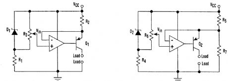


1. Though this setup can act as a cost-effective current source with an output accurate to 1%, the voltage offset will turn on the current source even when VCC equals Vin.2. Modifying the configuration of Figure 1 can rectify the problem of the current source being turned on by the voltage offset. The addition of R7 allows an adjustment that guarantees turn-off for any op-amp offset specification.
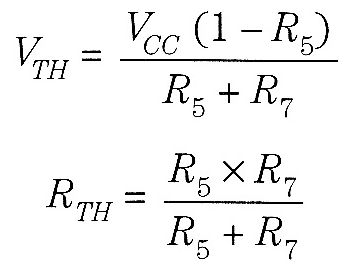
By carefully choosing components,you can create a cost effective circuit for a current Sourcewith an output that's accurate to 1%(Fig A). IOUT (the current flowing from the collector of Q1) is VCC-VIN(the voltage at the wiper of R3)divided by the value of R2.In some instances,it's important to be able to turn off the current source (within the limits of ICEO for Q1). Unfortunately, in about half of these cases,the offset voltage (Vos) of the op amp willturn the current Source on even when VCC=VIN That's because the offset voltage(when the norunverting input needs to be at a higher potential than the inverting input to get an output of 0V from the op amp) is impressed across R2 This offset voltage forces Q1 to turn on enough to yield a collector current of Vos divided by R2. Figure B offers a fix for this predicament The addition of R7 presents the emitter of Q2 with a Thevenin equivalent voltage and resistance represented by∶
The difference between VCC and VTH is VCC (R5/R5+R7) If VCC(R5/R5+R7) is set equal to the maximum Vos spec for the Op amp in question,the circuit is then guaranteed to turn off. This circuit hasan output current of VTH-VIN divided by RTHThe compromlse of Fig B does present another error term In the circuit The term (VTH-VIN)will have to be 2×VOS to guarantee a current output for whole population ofthe op amp chosen Thiserror can be made arbitrarily small (but not zero) by mcreasmg the voltage of D2 and VCC while raising the value of D2 and VCC while also ratsmg the value ofthe equivalent resistance RTH.
(View)
View full Circuit Diagram | Comments | Reading(679)
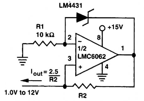
PRECISION_NEGATIVE_CURRENT_SOURCE
Published:2009/6/15 21:31:00 Author:May
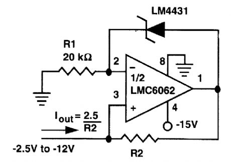
A National Semiconductor LM4431 reference and an LMC6062 op amp make up a negative cur-rent source. Current range is 1μA to 1mA. (View)
View full Circuit Diagram | Comments | Reading(707)
BILATERAL_CURRENT_SOURCE
Published:2009/6/15 21:30:00 Author:May
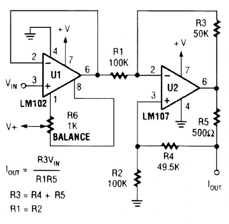
Using two op amps, this circuit produces current proportional to VIN (View)
View full Circuit Diagram | Comments | Reading(4)
PRECISION_POSITIVE_CURRENT_SOURCE
Published:2009/6/15 21:28:00 Author:May
An LM4431 precision 2.5-V reference and an LMC6062 op amp to make a positive current source, from 1mA to 10mA. (View)
View full Circuit Diagram | Comments | Reading(753)
CURRENT_SOURCE_FOR_LOW_RESISTANCE_MEASUREMENTS
Published:2009/6/15 21:27:00 Author:May
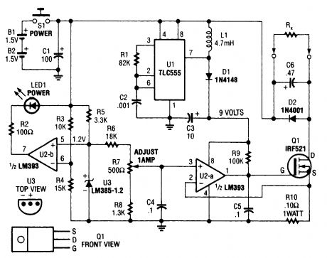


Useful for low-resistance measurements, this 1-A current source will produce 1 A in unknown resistance RX. For best results, RX should be less than 1 to 2Ω, because only 3V are available. U1 is a flyback converter to generate 9V for U2. (View)
View full Circuit Diagram | Comments | Reading(1811)
LOW_DROP_OUT_REGULATOR
Published:2009/6/23 4:06:00 Author:jailer
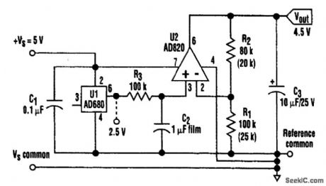
This low-dropout reference produces a 4.5-V output from a supply just a few hundred millivolts greater. With 1-mA dc Ioading, it maintains a stable 4.5-V output for inputs down to 4.7 V. (View)
View full Circuit Diagram | Comments | Reading(614)
5V 2A PC standby power supply circuit composed of TNY255P
Published:2011/5/16 4:59:00 Author:Rebekka | Keyword: PC standby power supply
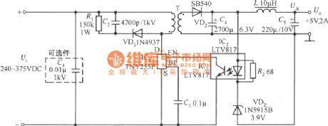
A 5V, 2A PC standby power supply circuit composed of TNY255P for PC is shown as above. Its input voltage Ui uses PC main power supply. The snubber circuit is composed of Rl, C2 and VDl. It can limit the spike voltage produced by TNY255P drain off mode in the safe range. The switching frequency of TNY255P is 130kHz. It is 3 times of TNY253P. So EE16 core can meet the standard of the 10W power output. The secondary voltage passes the VD2, C4, L and C5 rectifier filter and gains +5 V regulator output. (View)
View full Circuit Diagram | Comments | Reading(3027)
SBT-420AT Lightening Protection Socket
Published:2011/7/19 7:33:00 Author:Sue | Keyword: Lightening Protection, Socket
Functions and features:
SBT-420AT lightening protection socket has features of large current capacity, low residual voltage, over current insurance, high-frequency filtering. It uses advanced production technology. The lightening protection components all use brand-name products: the outer covering uses high-quality flame-retardant material;the socket components use high-quality phosphor bronze. (View)
View full Circuit Diagram | Comments | Reading(491)
Power Control Circuit When Computer Mainboard Is Started
Published:2011/7/20 7:40:00 Author:Sue | Keyword: Power Control, Computer Mainboard, Started

Starting Principle:
Before the power switch is pushed, PS-ON signal is pulled high by 5VSB voltage and will remain high level. PS-ON signal is P4 POWER's working control signal and when it is high level, P4 POWER doesn't work. When the switch is pushed, there will be a PWRBT# signal which will be sent to south bridge. The SLP-S3# signal output by south bridge is high level, which will control the triode Q33 to be connected. Then PS-ON signal of high level will be pulled low. PS-ON signal of low level will control POWER to output other working voltages 12V, -12V, -5V, VCC, VCC3. (View)
View full Circuit Diagram | Comments | Reading(828)
| Pages:180/291 At 20161162163164165166167168169170171172173174175176177178179180Under 20 |
Circuit Categories
power supply circuit
Amplifier Circuit
Basic Circuit
LED and Light Circuit
Sensor Circuit
Signal Processing
Electrical Equipment Circuit
Control Circuit
Remote Control Circuit
A/D-D/A Converter Circuit
Audio Circuit
Measuring and Test Circuit
Communication Circuit
Computer-Related Circuit
555 Circuit
Automotive Circuit
Repairing Circuit