
Index 195
HA17385 switching power supply with constant power
Published:2011/7/10 6:06:00 Author:chopper | Keyword: switching power supply, constant power
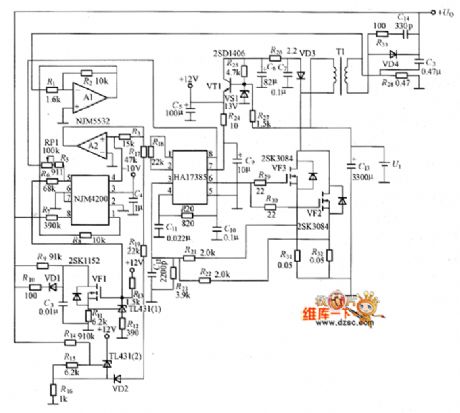
Figure shows HA17385 switching power supply with constant power,its output voltage is 85V (380V for no-load),output power is 35W, input voltage is 10~16V, and the maximum output current is about 0.5A.This constant switching power supply can be used for sputtering discharge,welding discharge systems and ballast which can inhibit radiation intensity of high-pressure mercury lamp.Circuit adopts on/off work method,the output power can be adjusted by RP1.
(View)
View full Circuit Diagram | Comments | Reading(1140)
UCC3580 converter circuit
Published:2011/7/10 5:49:00 Author:chopper | Keyword: converter circuit
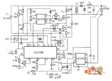
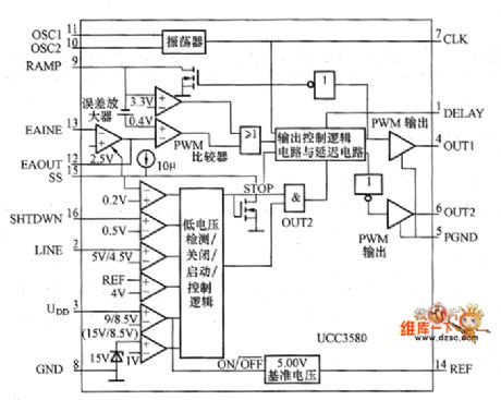
Figure 1 shows the UCC3580 converter, and it is the positive driving DC-DC converter whose input voltage is +18~+30 V, and output is 5V/8A. In the circuit, the control circuit adopts UCC3580 integrated controller,and the internal equivalent circuit is shown as Figure 2.In the UCC3580 there is the oscillator which can determine the switching frequency and dead time,error amplifier, pulse by pulse type over-current protection circuit,PWM control comparator,the circuit which can decide the work starting voltage and stopping voltage,and the PWM output which can drive the main switch and auxiliary switch and timing circuits and so on.
(View)
View full Circuit Diagram | Comments | Reading(965)
LT1725 converter circuit
Published:2011/7/10 5:37:00 Author:chopper | Keyword: converter circuit
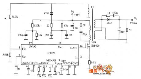
Figure shows the LT1725 converter,and this is the isolated DC-DC converter whose input voltage is +48V,and output is +5V/2A.As for the LT1725 integrated controller,it can obtain output voltage of high stability even if it is without negative feedback from the secondary side.And it has fewer external components,the circuit is relative simple.
(View)
View full Circuit Diagram | Comments | Reading(1524)
current limiting circuit
Published:2011/7/10 4:00:00 Author:chopper | Keyword: current, limiting circuit
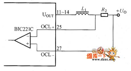
current limiting circuitis shown as picture
(View)
View full Circuit Diagram | Comments | Reading(596)
UC3843A converter circuit
Published:2011/7/10 5:32:00 Author:chopper | Keyword: converter circuit
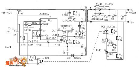
Figure shows the UC3843A converter,and it is the 5V/2A isolated flyback-type converter. This is the equivalent circuit of UC3843A whose input voltage is +36 ~+72 V,and output is shown as the picture.
(View)
View full Circuit Diagram | Comments | Reading(9277)
BIC1422 DC-AC converter circuit
Published:2011/7/10 3:59:00 Author:chopper | Keyword: DC-AC, converter circuit
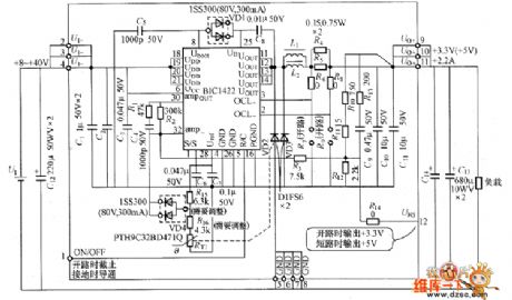
BIC1422 DC-AC converter circuit is shown as picture
(View)
View full Circuit Diagram | Comments | Reading(1047)
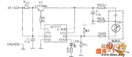
BQ2057 charger circuit uses the P-channel MOSFET design
Published:2011/7/10 18:52:00 Author:TaoXi | Keyword: charger, P-channel, MOSFET design
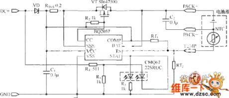
View full Circuit Diagram | Comments | Reading(820)
Practical lithium ion battery charger circuit composed of the MAX846A
Published:2011/7/10 18:54:00 Author:TaoXi | Keyword: Practical, lithium ion battery, charger
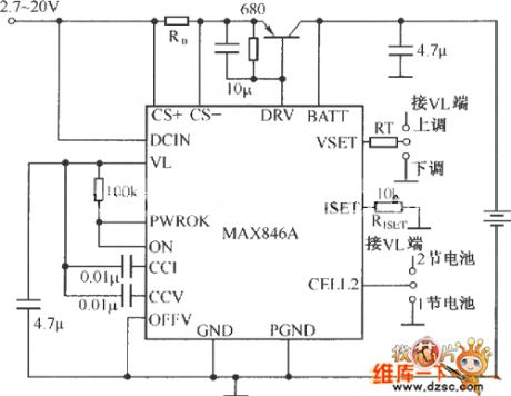
View full Circuit Diagram | Comments | Reading(756)
BQ2057 charger circuit uses the PNP transistor design
Published:2011/7/10 18:59:00 Author:TaoXi | Keyword: charger, PNP transistor
View full Circuit Diagram | Comments | Reading(952)
Blocking communication device power supply circuit uses the TDA4600
Published:2011/7/10 19:24:00 Author:TaoXi | Keyword: Blocking, communication device, power supply
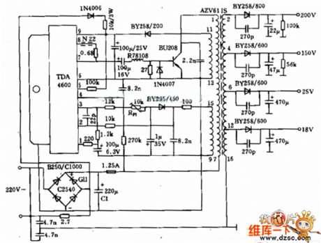
Figure:Blocking communication device power supply circuit uses the TDA4600
(View)
View full Circuit Diagram | Comments | Reading(2252)
Zero type rectifier voltage stabilization circuit
Published:2011/7/10 19:18:00 Author:TaoXi | Keyword: Zero type, rectifier, voltage stabilization
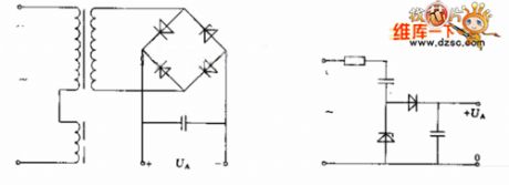
The circuit voltage regulator tube is connected with the capacitor and resistor components. The voltage regulator tube is connected with the AC power supply through the input capacitance in the conduction direction of it, and it limits the current in the blocking direction, so the rear capacitance recharges to stabilize the output voltage. This circuit has larger voltage pulse than the bridge type, and because the circuit is connected with the AC power supply directly, so the current consumption is small.
Figure:Zero type rectifier voltage stabilization circuit (View)
View full Circuit Diagram | Comments | Reading(679)
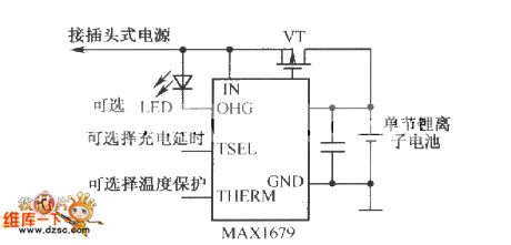
Charging circuit composed of the MAXl679
Published:2011/7/10 19:31:00 Author:TaoXi | Keyword: Charging circuit
View full Circuit Diagram | Comments | Reading(515)
Noise circuit diagram of processing feeble signal
Published:2011/6/16 23:59:00 Author:Sophia | Keyword: Noise circuit, Processing feeble signal
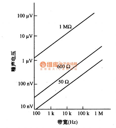
When designing the circuit of processing feeble AC signal, the key proplem of restricting performance is noise. The noise can be classified as three types: th ermal noise from signal source, the noise from the interior and exterior of electrical device. External noise has a transmission line noise, electrostatic noise coupling, electromagnetic coupling noise, radio noise and radiation, physical vibration, heat, light and other form of noise. Thermal noise is formed from the irregular movement of free electrons inside conductor. Thermal noise voltage Vn = 4KTRB, among which, K is Boltzmann constant (1.38x1O-23JK), T is thermodynamic temperature (K), R is the resistance value (Ω), B is the bandwidth product (HZ). From the above equation, thermal noise and the thermodynamic temperature, resistance, and bandwidth is proportional to the square root of the product. Thermodynamic temperature is calculated at T = 300.
. (View)
View full Circuit Diagram | Comments | Reading(596)
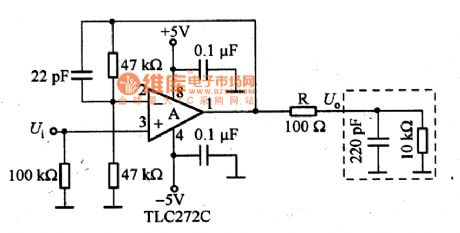
Processing on Capacitive loading circuit diagram
Published:2011/6/16 5:27:00 Author:Sophia | Keyword: Capacitive loading, Processing
(View)
View full Circuit Diagram | Comments | Reading(520)
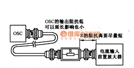
Small-signal circuit diagram under experiment circumstance
Published:2011/6/16 23:46:00 Author:Sophia | Keyword: Small-signal circuit, Under experiment circumstance
(View)
View full Circuit Diagram | Comments | Reading(500)
Input end protection circuit of dual power operational ampplifier
Published:2011/6/20 2:25:00 Author:Sophia | Keyword: Dual power operational ampplifier, Input end protection
(View)
View full Circuit Diagram | Comments | Reading(428)
Beijing City Hunter off-road vehicle non-contact ignition system and charging system circuit diagram
Published:2011/6/30 11:35:00 Author:Sophia | Keyword: Beijing City Hunter off-road vehicle, non-contact ignition system, charging system
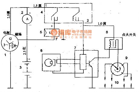
Non-contact ignition system (see Figure 1)
Non-contact ignition system BJ2020SG SUV circuit wiring diagram is shown in Figure 1. In addition to the ignition system suits, the rest of the circuit is unchanged. Non-contact ignition system circuit is shown in Figure 1. Rotor with four poles (with the same number of cylinders) and the stator winding signal generator coil, when the distributor shaft rotates, Non-contact ignition system produces the ignition signal four times a week, the signal voltage input to the ignition module 7. The electronic circuit is used to control turn on and off of the final stage switch tube, when the magnetic-electric ignition signal generator signal is not sent; the ignition coil primary current can flow through the last stage switch tube. When the ignition signal arrives, the last stage switch tube is cut-off, and turn off the primary current, so that the secondary coil generate high voltage, spark plug ignites. (View)
View full Circuit Diagram | Comments | Reading(653)
The package and internal structure circuit diagram of integrated chip S-8054ALR
Published:2011/7/7 5:58:00 Author:Sophia | Keyword: package, internal structure, integrated chip S-8054ALR
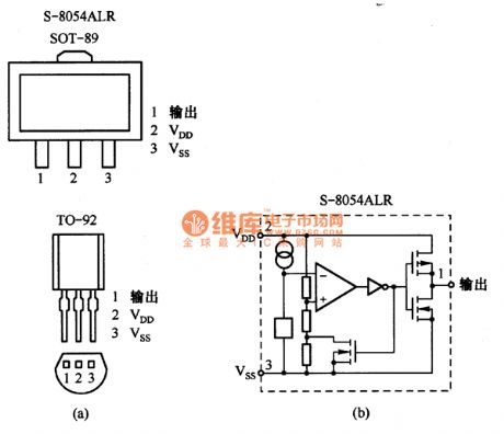
In order to obtain reliable reset signal, dedicated reset IC chips should be adopted. For example, integrated chip S-8054ALR, the package and the internal structure are showed as figure a and b, there are voltage reference and comparator inside the chip to make a comparision between UDD and the reference voltage (S-8054ALR integrated chip of the 4.3 ~ 4.6V) to output signal. (View)
View full Circuit Diagram | Comments | Reading(1346)
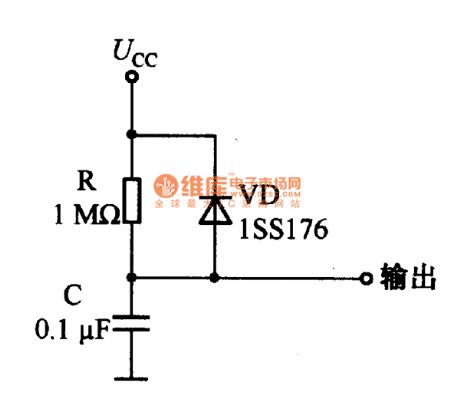
RC reset circuit diagram
Published:2011/7/7 6:19:00 Author:Sophia | Keyword: RC, reset circuit
(View)
View full Circuit Diagram | Comments | Reading(2748)
Part of Switching Power Supply Circuit
Published:2011/7/1 2:21:00 Author:Joyce | Keyword: Part , Switching Power Supply
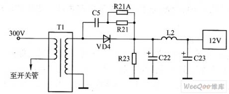
As shown in the figure, the 12 V voltage is not stable, therefore, the output part of the switching power supply should be examined first. Check whether the secondary winding of the switch transformer and VD4 function properly and make sure that inductance L2 has no cold solder joint. Parameters of filter capacitance C22 and C23 are 1000 pF / 16 V.If one uses the capacitance meter to measure C23, one will find that it works properly (capacity declines slightly), but the capacity of C22 drops to less than 80 uF. The reason is that the main source of the machine is installed at the base of the monitor, which is small and has low heat dissipation, while C23 and C22 both are close to the 12 V rectifier diode (especially C22), so their capacity would decline after baking, to lower the loading ability of the voltage, which further leads to this fault.
(View)
View full Circuit Diagram | Comments | Reading(492)
| Pages:195/291 At 20181182183184185186187188189190191192193194195196197198199200Under 20 |
Circuit Categories
power supply circuit
Amplifier Circuit
Basic Circuit
LED and Light Circuit
Sensor Circuit
Signal Processing
Electrical Equipment Circuit
Control Circuit
Remote Control Circuit
A/D-D/A Converter Circuit
Audio Circuit
Measuring and Test Circuit
Communication Circuit
Computer-Related Circuit
555 Circuit
Automotive Circuit
Repairing Circuit