power supply circuit
Single power supply switch plus or minus power circuit diagram
Published:2014/3/27 21:23:00 Author:lynne | Keyword: Single power supply switch plus or minus power circuit diagram, CD4069 | From:SeekIC
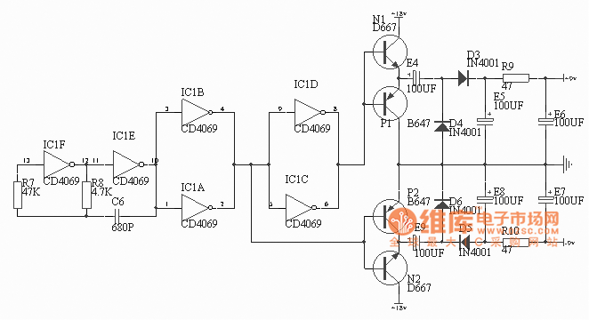
General Electric sound work, the need to provide positive and negative power. But in cars, boats, trains and other vehicles can only use battery power, a power supply circuit here, we want to help. The power from the oscillator circuit, inverter, rectifier and pusher and components such as filters, the circuit works as shown
Oscillator
This is a typical CMOS gate by (CD4069) constitute oscillator. Shock accuracy of 10-2 to 10-3, the shock process is as follows: Let the circuit at a time point B is high then the AB point to charge the capacitor through a resistor R8. The beginning of charging, the voltage across the capacitor is not due mutation, making the C point mutation to high potential, with the charge of conduct, C point potential gradually decreased. When the C-point conversion potential is lower than the voltage CMOS NAND gate, NAND gate 41F flip, A point goes high, B point becomes low. Since the voltage across the capacitor is not mutated, making the C point mutation to low potential. A point to the capacitor through a resistor R8 C6 reverse charge. With the charge carried, C point potential gradually increased when the C-point potential is higher than the conversion voltage CMOS NAND gate, NAND gate 41F flip, A point goes low, B point is to charge the capacitor through a resistor R8 C6 ...... repeating the above procedure, the formation of oscillation, the output pulse voltage at the point B. This oscillation frequency is f = 1/2ΠR8C6 = 1/2 * 3.14 * 4.7 * 103 * 680 * 10-12 = 49.8KHz, duty cycle 2. Figure resistor R7 (47K) Average value of R7 = (5 ~ 10) R8, its role is twofold: 1) to reduce the impact of power supply variations on the oscillation frequency. 2) reduce dynamic power circuits work.
Inverters
Divided into two groups of four inverters, respectively, opposite phase output pulse voltage, which pairwise parallel to increase the output current (SLR maximum output current of 1.5 mA, the shunt can output 3 mA). Advantages of CMOS inverters are: anti-interference ability, wide supply voltage range (3 ~ 20V), just apply to this circuit, the power of the circuit is 18V.
Pusher
Look at the two transistors N1 and P1 works, N1 consisting of common collector amplifier circuit for amplifying the input pulse voltage signal positive half cycle; P1 is also composed of common collector amplifier circuit for amplifying the negative half cycle of the input pulse voltage signal, they synthesized output phase with the input signal phase at point E, but opposite current amplification (up to two or three times) pulse voltage signal. Two transistors N2 and P2 with the working principle is similar, but the phase of the pulse signal and the voltage signal output from the point E to point F in opposite output, a rectifying circuit for the following positive and negative voltages, respectively, the entire effluent. In this circuit, the two transistors selection D647, D667, its argument is: 0.9w, +1 A/-1A.
Rectifier and filter
This part of the circuit is very classic, although voltage doubling rectifier circuit, but the loss due to other reasons, in this circuit when the load is +12 V/-12V, rated load +9 V/-9V. This power supply circuit provides power less than 11W.
Further, in the practical application of the circuit, the oscillation signal of the presence of 50KHZ, note frequency shielding, such as a printed board with this part of the circuit enclosed foil shielding. In addition, the power supply ripple factor depending on the desired single-supply ripple. Since the commissioning of the project power is not available, so long as the part is good, the connection is correct, it can work properly.
Single power converter shown in Figure positive and negative power supply circuit
Reprinted Url Of This Article:
http://www.seekic.com/circuit_diagram/Power_Supply_Circuit/Single_power_supply_switch_plus_or_minus_power_circuit_diagram.html
Print this Page | Comments | Reading(3)

Article Categories
power supply circuit
Amplifier Circuit
Basic Circuit
LED and Light Circuit
Sensor Circuit
Signal Processing
Electrical Equipment Circuit
Control Circuit
Remote Control Circuit
A/D-D/A Converter Circuit
Audio Circuit
Measuring and Test Circuit
Communication Circuit
Computer-Related Circuit
555 Circuit
Automotive Circuit
Repairing Circuit
Code: