Switching-Regulator Circuit
Buck chopped wave switching power supply circuit diagram
Published:2011/3/24 21:42:00 Author:Nicole | Keyword: switching power supply | From:SeekIC
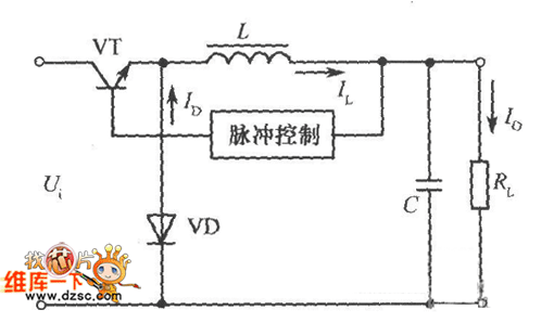
This is a buck chopped wave switching power supply circuit diagram. When the switching element VT is controlled as saturated conduction, the energy is stored in inductor L and capacitor C, and also is fed to the load. When the switching element VT is controlled as cut-off state, the energy stored in inductor and capacitor continue to supply the load, the diode VD constitute a current loop. Because of the switching element VT in series with the load resistor RL, so it is called series switching power supply.
Chopped wave switching power supply is a DC power supply, can obtain unidirectional square wave from switch circuit, and then can get a different steady DC which is different from the input voltage after filtered. The buck is whether the input voltage Ui is positive or negative, the output voltage Uo is always lower than the input voltage Ui, that is | Uo | ≤ | Ui |.
If the adjustment switching element VT has been conducting, the off-time is zero, then Uo = Ui; if VT has been cut-off, on-time is zero, then Uo = 0V. As the ratio of ton and toff is different, the output voltage Uo is between O ~ Ui.
Reprinted Url Of This Article:
http://www.seekic.com/circuit_diagram/Power_Supply_Circuit/Switching-Regulator_Circuit/Buck_chopped_wave_switching_power_supply_circuit_diagram.html
Print this Page | Comments | Reading(3)

Article Categories
power supply circuit
Amplifier Circuit
Basic Circuit
LED and Light Circuit
Sensor Circuit
Signal Processing
Electrical Equipment Circuit
Control Circuit
Remote Control Circuit
A/D-D/A Converter Circuit
Audio Circuit
Measuring and Test Circuit
Communication Circuit
Computer-Related Circuit
555 Circuit
Automotive Circuit
Repairing Circuit
Code: