Basic Circuit
The current loop interface circuit diagram of AD694 being used as D / A converter
Published:2011/9/18 22:35:00 Author:Ecco | Keyword: current loop , interface circuit, D / A converter | From:SeekIC
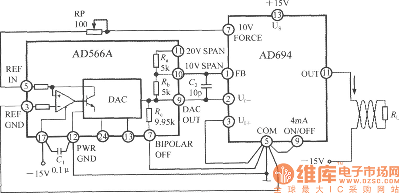
The current loop interface circuit diagram of AD694 multi-functional sensor signal conditioner being used as D / A converter.
The current loop interface of AD694 being used as D / A converter (DAC) can achieve the conversion of digitalvalue →voltage signal →current signal . DAC's current loop interface circuit is shown as the chart. AD566A is high-speed 12-bit DAC, its output (DAC OUT) is connected to AD694's UI-end, UI + is grounded. AD694 uses ± 15V dual supplies, and provides reference voltage to the AD566A. Internal resistor network of AD566A will set AD694 with 10V full scale input. C2 is the frequency compensation capacitor. RP is the full scale adjusting potentiometer, it has no need to use a fixed adjustment 50Ω resistor to replace the potentiometer.
Reprinted Url Of This Article:
http://www.seekic.com/circuit_diagram/basic_circuit/the_current_loop_interface_circuit_diagram_of_ad694_being_used_as_d___a_converter.html
Print this Page | Comments | Reading(3)

Article Categories
power supply circuit
Amplifier Circuit
Basic Circuit
LED and Light Circuit
Sensor Circuit
Signal Processing
Electrical Equipment Circuit
Control Circuit
Remote Control Circuit
A/D-D/A Converter Circuit
Audio Circuit
Measuring and Test Circuit
Communication Circuit
Computer-Related Circuit
555 Circuit
Automotive Circuit
Repairing Circuit
Code: