
Index 211
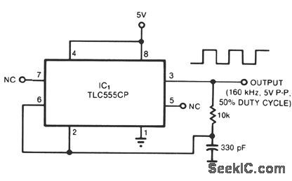
SQUARE_WAVE_PULSE_EXTRACTOR
Published:2009/7/10 2:36:00 Author:May
This circuit traps a single positive pulse from a square-wave train. Following the rising edge of an input command, the pulse-out signal emits a replica of one positive pulse of the clock signal simultaneous with the clock signal's next rising edge. The input command signal sets the Q1 output of flip-flop IC1A. Consequently, the next rising edge of the clock signal sets the Q2 output of IC1B, which allows AND gate IC2C to pass the clock signal's next positive pulse. AND gates IC2A and IC2B prevent the generation of brief output glitches by delaying the clock signal by tD seconds (two propa-gation delays). (View)
View full Circuit Diagram | Comments | Reading(803)
PRECISION_PHASE_SPLITTER
Published:2009/7/10 2:33:00 Author:May
View full Circuit Diagram | Comments | Reading(1104)
SIMPLE_ABSOLUTE_VALUE_CIRCUIT
Published:2009/7/10 2:33:00 Author:May
When an input voltage is positive, the output of ICA is negative and diode D does not conduct; hence the output of ICB is positive. On the other hand, when the input is negative, the output of ICA is positive.D will conduct and cause the absolute value, expressed as a positive voltage, to appear on the noninverting input of ICB and on the circuit's output.
The circuit'sdynamic range extends from zero to the point at which the op amp saturates. The band-width is determined by the characteristics of the diode and the high-frequency performance of the op amp. (View)
View full Circuit Diagram | Comments | Reading(1280)
WIDEBAND_SIGNAL_SPLITTER
Published:2009/7/10 2:33:00 Author:May
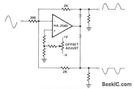
With one HA-2539 or HA-2540 and two low-capacitance switching diodes, signals exceeding 10 MHz can be separated. This circuit is most useful for full-wave rectification, AM detection, or sync generation. (View)
View full Circuit Diagram | Comments | Reading(624)
SIMPLE_DIODE_CURVE_TRACER
Published:2009/7/10 2:31:00 Author:May
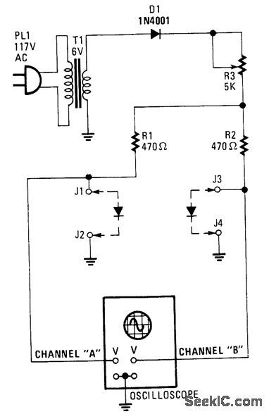
Suitable for matching diodes or examining V/I characteristics of two terminal devices (diodes, etc.), this circuit should be handy for lab use. R1 and R2 can be increased in value and a higher voltage transformer can be used for higher voltage test using this principle. (View)
View full Circuit Diagram | Comments | Reading(768)
OCTAVE_SHIFTER_FOR_MUSICAL_EFFECTS
Published:2009/7/10 2:31:00 Author:May
This musical special-effect device is basically a frequency doubler. The input audio is amplified and doubled by using a full-wave rectifier, which has a dc output plus a twice the ac frequency component. The 2 x frequency component is fed to the output. (View)
View full Circuit Diagram | Comments | Reading(951)
STABLE_SUPERREGENERATIVE
Published:2009/7/10 2:30:00 Author:May
Agc circuit transforms grid-pulsed superregenerative am pliler V1 into noncritical circuit that is stable for long periods when controlled by pulse generator V4-V5, which in tum is controlled by extemal trigger pulse source.-J. H. Kuck, Automatk Gain Control for Superregenerative Amplifiers, Electronics, 34:29, p 76-79. (View)
View full Circuit Diagram | Comments | Reading(489)
VOR_SIGNAL_SIMULATOR
Published:2009/7/10 2:29:00 Author:May
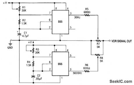
An output of 9960 and 30 Hz at 0.5 Vrms is produced by this VOR (VHF Omni Range) signal simula-tor, which uses a pair of 555 timers. Alternatively, a 556 (two timers in one package) could be used. (View)
View full Circuit Diagram | Comments | Reading(685)
LOW_COST_BAROMETER
Published:2009/7/10 2:28:00 Author:May
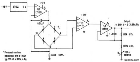
Using Linear Technology LT1027 reference and LT1078 op amps, transducer T1 is fed with 1.5mA.The pressure transducer feeds an amplifier with a gain of 10, then it feeds a voltage follower. Output can either drive an analog meter or a DVM circuit. (View)
View full Circuit Diagram | Comments | Reading(1123)
MUSICAL_DOORBELL
Published:2009/7/10 2:27:00 Author:May
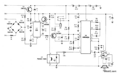
8 to 15 Vac is applied to terminals C and D,which produces a dc voltage across R2, and turns on Q1.This connects the batteries B1 and B2 to the rest of the circuit,which activates it.Latch U3 is triggered,it remalns on until Q2 turns on,charges C2,and turns off U2.When U3 is turned on,Q3 is forward-biased,which energlzes K1,powers up U4.At the time the K1 contacts close,C4 couples a positive spike to pin 4 of U4,a melody synthesizer chip.U4 generates a pre-programmed tune,at the end of which pin 1 of U4 goes positive,This activates optocoupler U1 and turns off Q2,which drops out the relay.U2 acts as an audio amplifier, which drives an 8-Ω speaker. (View)
View full Circuit Diagram | Comments | Reading(1151)
Basic_digital_thermometer
Published:2009/7/19 21:53:00 Author:Jessie
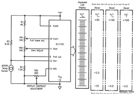
This circuit shows an ICL7182 bargraph converter that is connected to form a basic digital thermometer, with a bargraph readout. The connections between the ICL7182 and bargraph are shown in Fig. 12-14. Harris Semiconductors Data Acquisition.1991 p 2-145 (View)
View full Circuit Diagram | Comments | Reading(1188)
RACE_CAR_MOTOR_CRASH
Published:2009/7/10 2:27:00 Author:May
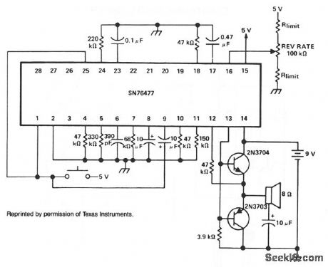
For two simultaneous race-car sounds, the mixer can be multiplexed between the SLF and VCO functions. (View)
View full Circuit Diagram | Comments | Reading(460)
100_KHz_CRYSTAL_CALIBRATOR
Published:2009/7/10 2:27:00 Author:May
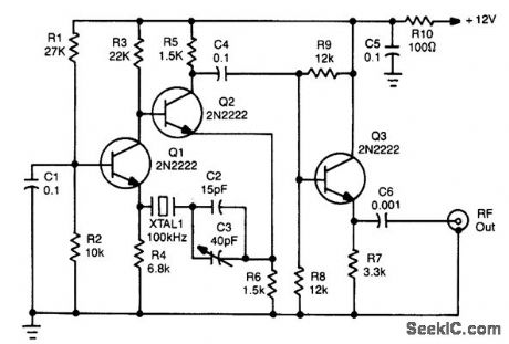
Using a 12-V supply, this crystal calibrator should prove a useful accessory for a SW receiver. Q1 and Q2 form an oscillator and Q3 is a buffer amp. (View)
View full Circuit Diagram | Comments | Reading(1885)
ELECTRONIC_BIRD_CHIRPER
Published:2009/7/10 2:26:00 Author:May
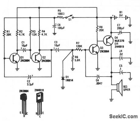
Transistors Q1 and Q2 form the two halves of a free-running multivibrator whose frequency is determined by the voltage across C8. That capacitor is charged and discharged by closing and opening switch S1. Transistors Q3 and Q4 make up a VFO. The output of the free-running multivibrator frequency modulates the Q3/Q4 oscillator, causing the chirping bird sound. The number of chirps per second is determined by the frequency of the Q1/Q2 multivibrator, which also varies. The pitch of the chirps is determined by C5 and C6. (View)
View full Circuit Diagram | Comments | Reading(1242)
B_FIELD_MEASURER
Published:2009/7/10 2:26:00 Author:May
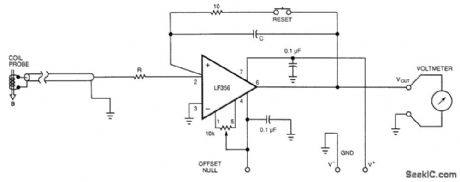
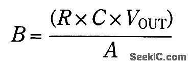
This circuit develops an output voltage that is proportional to the magnetic induction, B, flowing through its probe's coil. You must size the coil to give a full-scale, 10-V output for your maximum expected magnetic-induction intensity.
For a given value of B (in tesla) and output voltage, VOUt:
where A is the effective area or your coil in m2 (A = number of turns × average area of each turn), R is the resistance of the coil and the probe, and C is the value of the capacitor. Notice that C should be a low-leakage polypropylene or Teflon device.
For most practical applications that measure a magnetic field in the air, the coil will be either tiny or very thin. If R=1kΩ, C=1μF, and the coil is 100 turns with a mean area per turn of 1 cm2, then the circuit's output will be 1 mV/gauss (1T= 104G).
To use the circuit, push the reset button and place the probe in an area that you know is devoid of magnetic fields. Be sure to avoid magnets and iron. Then, put the probe into the field to be measured and read the V0UT with a voltmeter. Finally, calculate the B field's intensity using the equation.
When constructing the instrument, guard the op amp's inputs from undesirable currents at the minus input. For full-scale outputs, use a ±15-V supply for the op amp. (View)
View full Circuit Diagram | Comments | Reading(515)
TEMPERATURE_COMPENSATED_DARLINGTON
Published:2009/7/10 2:23:00 Author:May

Modiled Darlington includes two diodes and additional resistor. With these, temperature changes up to 50℃ have no effect on output.-R. C. Going, Tempercature-Stctbilized Darlington, EEE, 11:7, p 28-29. (View)
View full Circuit Diagram | Comments | Reading(511)
CHUG_CHUG
Published:2009/7/10 2:23:00 Author:May
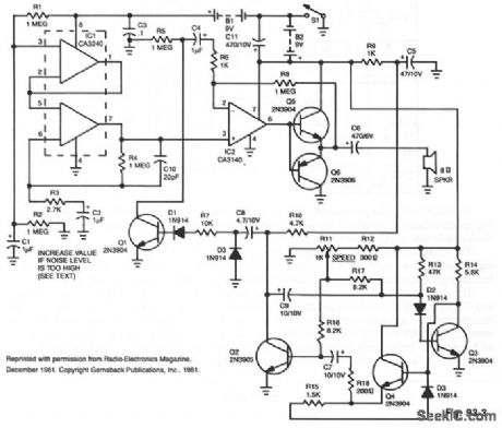
A CA3240 dual MOSFET-input device is used as a white-noise source. Op amp IC2 is used as a driver stage for the push-pull output stage formed by Q5 and Q6. Transistors Q2, Q3, and Q4 form a variable-frequency multivibrator. R11, the speed control, is used to control the multivibrator's frequency. The output is differentiated by C8 and applied to modulator transistor Q1, through D1 and R7. Transistor Q1 modulates the gain of the output amplifier stage by changing the impedance to ground, through R6 and C4.When the multivibrator's frequency is reduced using R11, C8 discharges slowly, creating a sound similar to escaping steam from a stopped locomotive.To find the proper value for R3, short Q1's collector to ground. Then, increase the value of R3 until the current drain from the power supply is less than 60 mA. Then remove the short from Q1. To see if the device is operating properly, close switch S1 and reduce the resistance of R11. Wait 10 seconds, then rotate R11 slowly. You should hear a sound similar to a steam locomotive picking up speed. (View)
View full Circuit Diagram | Comments | Reading(636)
160_MC_750_MW_POWER_STAGE
Published:2009/7/10 2:22:00 Author:May
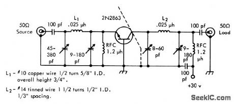
Pi matching networks at input and output optimize tronsistor performonce in class C operation. Ef-ficiency is 25% snd 3-db bandwidth is 15 Mc,Texas Instruments Inc., solid-State Communications, McGraw-Hill, N.Y., 1966,p 318. (View)
View full Circuit Diagram | Comments | Reading(503)
ELECTRONIC_MUSIC_MAKER
Published:2009/7/10 2:20:00 Author:May

This electronic muslc maker uses an astable oscillator circuit that is controlled by a photocell.Thelight falling on the photo cell controls the tone.By mounting the circuit h a box,you can control lightreading PC1 with your hand. (View)
View full Circuit Diagram | Comments | Reading(670)
FUZZ_BOX
Published:2009/7/10 2:20:00 Author:May
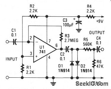
The 741's maximum gain of 20,000 is pushed to nearly 3 million dB, and therefore distorts the output. That distortion provides the fuzz sound.The level is dropped by clipping the two diodes. (View)
View full Circuit Diagram | Comments | Reading(2002)
| Pages:211/471 At 20201202203204205206207208209210211212213214215216217218219220Under 20 |
Circuit Categories
power supply circuit
Amplifier Circuit
Basic Circuit
LED and Light Circuit
Sensor Circuit
Signal Processing
Electrical Equipment Circuit
Control Circuit
Remote Control Circuit
A/D-D/A Converter Circuit
Audio Circuit
Measuring and Test Circuit
Communication Circuit
Computer-Related Circuit
555 Circuit
Automotive Circuit
Repairing Circuit