
Automatic Control
Index 3
A bean sprouts automatic watering controller consisting of 555 circuit
Published:2011/7/8 2:20:00 Author:Fiona | Keyword: automatic watering controller
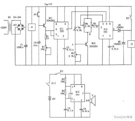
Figure shows the bean sprouts automatic watering control circuit. The controller consists of step-down rectifier circuit, power outage told implement (IC3), timing control circuit (IC1), temperature control circuit(IC2) and so on. The step-down rectifier circuit is VDD = +7 V DC voltage provided by the whole controller. The power outage told implement is controlled by many harmonic oscillator which consists of IC3,R3,R4,C5 and other components. Close the switch K1, when the power cuts, the relay J1 releases, contact J1-1 closes, IC3 starts oscillation due to get electricity, the oscillation frequency is about 1000Hz, the output signal drives the speaker sound to inform the owner that the power goes out. (View)
View full Circuit Diagram | Comments | Reading(1283)
a TV set automatic shutdown control circuit consisting of 555
Published:2011/7/8 2:18:00 Author:Fiona | Keyword: automatic shutdown control
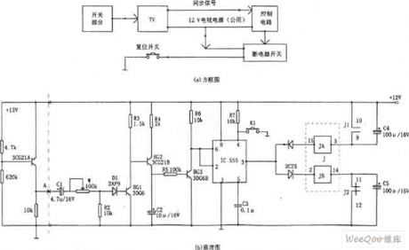
When there is a television program,the sync signal from point A makes BG1 saturated conduct,BG2, BG3 conducts, so that 555 is set due to thepin ② is low level, the high level output by ③ feet makes JB put together, J1 is closed and the TV power supply connects up; when the television program is aired, synchronous signal disappears, BG1, BG2 end.C2 which has been charged discharges through the emitter of R5, BG3 and makesBG3 stay about 10 minutes conducting timeto avoid the undue off phenomenon caused by intermittent or replacement when program broadcasts. (View)
View full Circuit Diagram | Comments | Reading(731)
Timing Controller (the 1st)
Published:2011/7/7 22:29:00 Author:Felicity | Keyword: Timing Controller
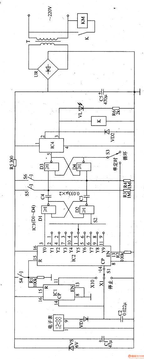
Work of the circuit
The circuit consists of Power supply circuit, the clock signal generator, counting distributor circuit, flip-flop circuit and control output circuit. (It is showed in picture 8-90.)
Power supply circuit consists of Power transformer T, bridge rectifier, UR, filter capacitor Cl, C5, current limiting resistor R5 and Zener VS.
The clock signal generator consists of electronic clock, diodes VDl, capacitor C2 and the count divider integrated circuit ICl.
Counting distributor circuit consists of count divider integrated circuit IC2, resistors Rl, R2, timer selection switch Sl, S2 and reset button S4.
Flip-flop circuit consists of NAND gate integrated circuit IC3 (Dl-D4) and capacitor C3, C4, resistor R3, R4, the Close button S5, S6 on the button and loop / single timer switch S3.
Control output circuit consists of electronic switch integrated circuit IC4, diode VD2, relay K, light-emitting diode VL, resistors R6 and AC contactor KM. (View)
View full Circuit Diagram | Comments | Reading(741)
Timing Controller (the 6th)
Published:2011/7/7 22:34:00 Author:Felicity | Keyword: Timing Controller (the 6th)
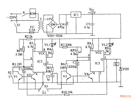
Work of the circuit
The circuit consists of power circuit, timing control circuit and control implementation circuit. (It is showed in picture 8-95.)
Power circuit consists of power switch Sl, fuse FU, power transformer T, rectifier diode VDl-VD4, filter capacitor C4, C5, and three-terminal regulator IC lCl.
Timing control circuit consists of time-base integrated circuit IC2, 1C3, resistors Rl-RlO, capacitors Cl-C3, potentiometer RPl, RP2, transistor Vl-V4, LED VL1, VL2, manual discharge button function selector switch S2 and S3.
Control implementation circuit consists of diode VD5, relay K and AC contactor KM. (View)
View full Circuit Diagram | Comments | Reading(719)
Timing Controller (the 5th)
Published:2011/7/7 22:33:00 Author:Felicity | Keyword: Timing Controller
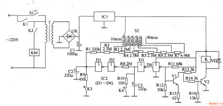
Work of the circuit
The circuit consists of power regulator circuit, timing time circuit, delay circuit and Schmitt trigger control circuit. (It is showed in picture 8-94.)
Power regulator circuit consists of start button SI, power transformer T, bridge rectifier, UR, filter capacitors Cl and three-terminal voltage regulator integrated circuit ICl.
Timing time circuit consists of selector switch S2 and resistors Rl-R7.
Delay circuit consists of capacitors C2, C3, resistors R9, RlO, the normally closed contact relay K K3, K4 and non-gate integrated circuits IC2 (D1-D4).
Schmitt trigger control circuit consists of transistor Vl, V2, resistors RI-R16 and diode VD. (View)
View full Circuit Diagram | Comments | Reading(672)
Timing Controller (the 4th)
Published:2011/7/7 22:31:00 Author:Felicity | Keyword: Timing Controller
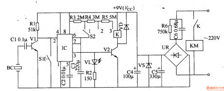
Work of the circuit
The circuit consists of power circuit, the input control circuit, timing circuit and output control circuit. (It is showed in picture 8-93.)
Power circuit consists of Buck capacitor C6, discharge resistors R6, bridge rectifier, UR, filtering capacitor C5, C4 and Zener VS.
The input control circuit consists of the piezoelectric ceramic BC on Electronic alarm clock, capacitor Cl, resistors Rl and transistor Vl.
Timing circuit consists of Resistors Rl-R5, reset button, Sl, regular timing switch S2, capacitor C2 and C3, light-emitting diode VL and time -based integrated circuit IC.
Output control circuit consists of transistor V2, the relay K, the diode VD and AC contactor KM. (View)
View full Circuit Diagram | Comments | Reading(689)
Timing Controller (the 3rd)
Published:2011/7/7 22:30:00 Author:Felicity | Keyword: Timing Controller
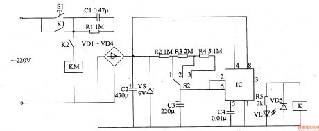
Work of the circuit
The circuit consists of power circuit and timing control circuit. (It is showed in picture 8-92.)
Power circuit consists of Power control button Sl, the normally open relay contact K Kl, step-down capacitor Cl, discharge resistors Rl, rectifier diode VDl-VD4, filter capacitor C2 and Zener VS.
Timing control circuit consists of Time-base IC lC, delay selector switch S2, resistors R2-R5, capacitor C3, C4, light-emitting diode VL, relay K and diode VD5. (View)
View full Circuit Diagram | Comments | Reading(774)
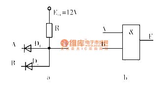
The input and output protection circuit of digital integreted circuit
Published:2011/7/7 7:32:00 Author:Sophia | Keyword: Input and output, protection circuit, digital integreted circuit
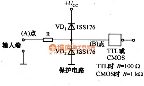
Signal low level UIL of TTL circuit is less than or equal to 0.8V, high UIH is great than or equal to 2.0v. If external digital signal level it receives is within this range, there will be no proplem. In the actual circuit, due to various reasons, the input signal level will be high. Therefore, the input of the digital circuit should be protected from the circuit damaged. Figure is the most common protection circuit. In this circuit, the resistor R is the current limiting resistor, and diode VD1 and VD2 are used to limit the input signal level of digital circuit. The greater R-value, the better the protection, but the voltage drop on input current will be greater. Therefore. For TTL circuits, R should be 100Ω; for CMOS circuits, R is 1kΩ,which will be more appropriate.
(View)
View full Circuit Diagram | Comments | Reading(1833)
ground isolation circuit by optical couplers
Published:2011/7/4 23:44:00 Author:chopper | Keyword: ground isolation, optical couplers
As for some circuits,one point connection between AGND and DGND is very different.Additionally,because of the difference of electric potential of the AGND and DGND in the circuit,the landlines can't be connected.And we adopts optical coupler to separate the AGND and DGND,just as picture.If the signal is transfered in the form of light,then the connection between AGND and DGND is not necessary.
(View)
View full Circuit Diagram | Comments | Reading(587)
example of A/D and D/A converter circuit
Published:2011/6/27 10:00:00 Author:chopper | Keyword: example, A/D and D/A, converter
The picture is the typical instance of digital analog circuit,and it is a A/D and D/A converter circuit.The A/D and D/A integrated chip is on the edge of the digital circuit and analog circuit.Thus,these chips include AGND and DGND,and there is no current going through the ground,the leads need not too thick.
(View)
View full Circuit Diagram | Comments | Reading(617)
landlines of digital and analog circuit on the same placode circuit
Published:2011/6/27 10:13:00 Author:chopper | Keyword: landlines, digital and analog circuit, same placode

When the digital circuit and analog circuit are on the same placode,the trend of the landlines is very important to prevent the noise of digital circuit from mixing into the analog circuit to effect its performance.The digital circuit and analog circuit must be separated physically if they are on the same circuit,because the analog ground AGND and digial ground DGND should be separated definitely.AGND and DGND should be connected at one point,just as picture a,b.
(View)
View full Circuit Diagram | Comments | Reading(596)
power supply and landlines of digital circuit
Published:2011/6/27 21:07:00 Author:chopper | Keyword: power supply, landlines, digital circuit
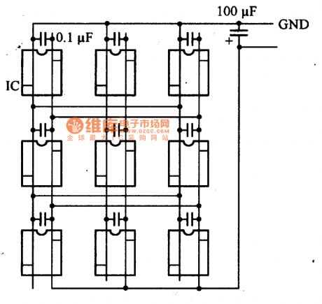
As to digital circuit,the impedance of power supply should be low as possible as we can.The high impedance will effect the circuit.The picture is a connection method of double-sided printed circuit board.On the element installation surface there are horizontal and longitudinal leads,and leads should be short and thick as possible as we can.Additionally,the leads are in grid shape to reduce the circuit impedance when the frequency is high.The waxy capacitance of power supply can reduce the high frequency impedance of leads of power supply.Thus,every IC is connected with a 0.1μF ceramic capacitor.To reduce the low frequency impedance of leads of power supply,we can add a 100μF electrolytic capacitor to the input end of power supply.
(View)
View full Circuit Diagram | Comments | Reading(617)
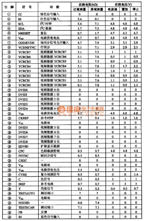
TAl218N video,audio converting switch integrated circuit
Published:2011/6/16 22:45:00 Author:chopper | Keyword: video,audio, converting, switch integrated circuit
TAl218N is a video/audio converting switch circuit,and it is applied to homemade and import large-screen colour TVs widely.1.function characteristicsTAl218N integrated circuit includes I2C bus interface circuit,main/sprite video signal switching circuit,TV/AV audio switching circuit,Y/C separation signal switching circuit,TV video/audio switching circuit,sub-audio,flare,luminance signal switching circuit,L/H,U/V frequency band switching circuit,and other miscellaneous function circuits.
(View)
View full Circuit Diagram | Comments | Reading(662)
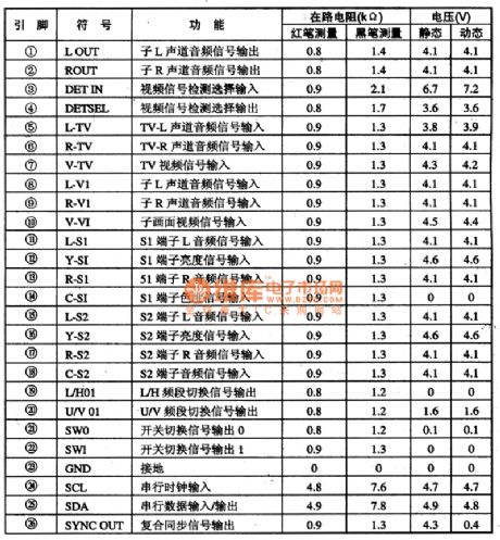
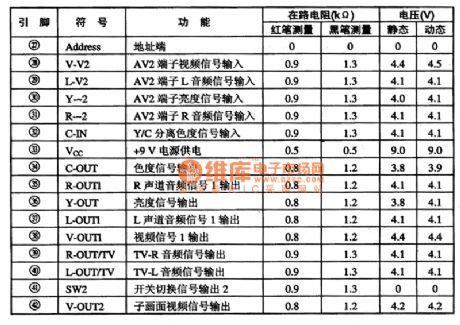
STVO117A digital video coding integrated circuit
Published:2011/6/14 9:16:00 Author:chopper | Keyword: digital video, coding, integrated circuit
STVO117A is a digital video coding integrated circuit produced by French Company SGS-THOMSON and it is applied to various homemade and import DVD players.1.function characteristicsSTVO117A integrated circuit adopts I2C bus-mastering,and it can code input 8bit or 16bit video data stream into analog composite video signal or S video Y/C signal.It includes multipath output selector,matrixing circuit,modulator,caption generator,color sub-carrier combiner circuit and clock sync generator,three 9bit DAC circuit and IC2 bus interface circuit.2.function and data of pinsSTV0117A integrated circuit adopts single inline package.The function and data of pins of integrated circuit are shown as chart 1.
(View)
View full Circuit Diagram | Comments | Reading(640)
TTL integrated door circuit
Published:2011/6/16 1:10:00 Author:chopper | Keyword: TTL, integrated door
View full Circuit Diagram | Comments | Reading(572)
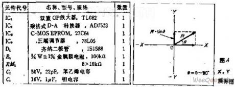
achieving multiply the analog input and digital data R.SINθ conversion circuit
Published:2011/5/12 5:06:00 Author:Fiona | Keyword: achieving multiply the analog input and digital data, R.SINθ conversion
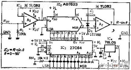
Circuit function
he circuit outputs Y (Y = R. SINθ) function (in Figure A,X, Y is as coordinates, R is representative of the analog input, Y is representative of the function output),θ's selected range is 0 to 90 degrees.90 to 180 degrees and 0 to 90 happens is reciprocal.To make the data can wait until 180 degrees, the control signal uses two BCD code +1 data bits.
Circuit Work
This is an analog input and digital data multiplication circuit which does the R computing and the digital data values is from 0 to 255.In advance, make the ROM data corresponding to the sine function good,because AD7523 is a positive logic input,SIN0 degree = 0, D = 00; SIN90 degree = 1, D = FFH (255/255 ≈ 1).Calculate SIN0 ~ 90 degrees to a degree level,then multiply by 25and switch to binary data to store in the P-ROM.
(View)
View full Circuit Diagram | Comments | Reading(750)
counter circuit
Published:2011/6/8 20:51:00 Author:chopper | Keyword: counter
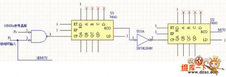
Measuring phase angle adopts hardware counting mode instead of singlechip direct counting mode.Because hardware counting mode can improve the precision.We make 256 scale successive carry counting mode by using two pieces of 74HC161 in series.The external frequency reference selects a high-speed pulse generated by 10MHz active crystal oscillator to count the width of signal Fi output by phase-locked loop.Therefore,it can make the measuring absolute error of transadmittance angle less than 5% of theoretic calculation.The principle of circuit is as follows.
(View)
View full Circuit Diagram | Comments | Reading(620)
MAX038 inside casing circuit
Published:2011/6/8 8:02:00 Author:chopper | Keyword: inside casing
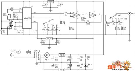
Frequency in every frequency band is controlled by RP1 and RP2.RP1 is coarse adjustable potentiometer.The charge current of oscillating capacitor CF is changed by altering the value of RP1 in order tochange the frequency.RP2 is fine tuning potentiometer,and it changes output frequency by changing the value of UFADJ.The variation range of RP2 is not great,and it is usedas a vernier regulation.The dutyfactor of every waveform is fixed as 50% so that can simplify the circuit.This has been able to satisfy many occasions. (View)
View full Circuit Diagram | Comments | Reading(3211)
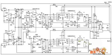
LM1875 current feedback BTL circuit
Published:2011/6/3 20:12:00 Author:chopper | Keyword: current feedback, BTL

View full Circuit Diagram | Comments | Reading(3316)
Negative feedback circuit of Pure dc current made by LM3886
Published:2011/6/2 5:49:00 Author:chopper | Keyword: Negative feedback circuit, Pure dc current
LM3886 is of excellent performance and win its popularity on sound system in recent years.Many power amplifiers use it as the latter stage amplifier or supper bass amplifying circuit directly. It uses LM3886TF as power amplifier which is a new hi-fi stereo amplifier integrated circuit produced by US company NS(a semiconductor company of State) and uses operational amplifier NE5532 or AD827 as leading linear amplifier and tone amplifier.
(View)
View full Circuit Diagram | Comments | Reading(3378)
| Pages:3/5 12345 |
Circuit Categories
power supply circuit
Amplifier Circuit
Basic Circuit
LED and Light Circuit
Sensor Circuit
Signal Processing
Electrical Equipment Circuit
Control Circuit
Remote Control Circuit
A/D-D/A Converter Circuit
Audio Circuit
Measuring and Test Circuit
Communication Circuit
Computer-Related Circuit
555 Circuit
Automotive Circuit
Repairing Circuit