
Other Circuit
Index 3
The frequency divider circuit with a rate of 34 and made by CD4017
Published:2011/8/14 7:14:00 Author:leo | Keyword: Frequency divider, rate
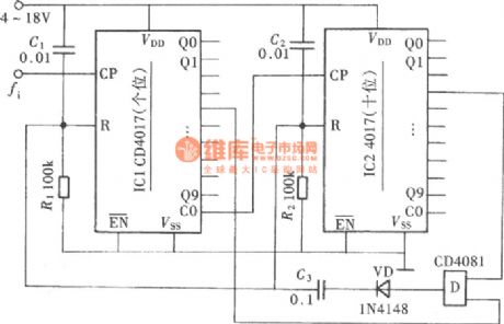
The frequency divider is formed by two CD4017 and dual input port. It can expand the frequency rate to 2 to 99 through different combinationsand connection, which is shown as following: (View)
View full Circuit Diagram | Comments | Reading(2395)
The frequency lock indicator formed by CD4046
Published:2011/8/14 7:17:00 Author:leo | Keyword: Frequency lock, indicator
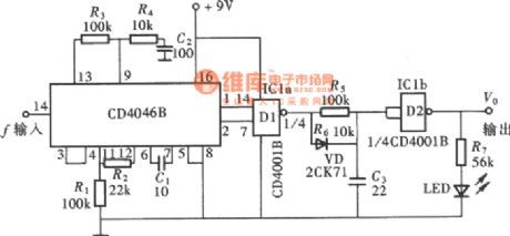
It can design a frequency lock indicator based the output features of two phase compatators of the lock circuit under the condition of locking frequency. (View)
View full Circuit Diagram | Comments | Reading(2413)
The sweeping signal generator formed by CD4046
Published:2011/8/14 7:27:00 Author:leo | Keyword: Sweeping signal, generator
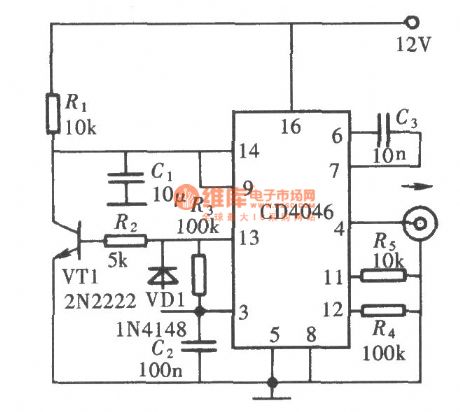
View full Circuit Diagram | Comments | Reading(2624)
MC3406A reversible DC-DC convetor
Published:2011/8/11 11:15:00 Author:leo | Keyword: Reversible feature, DC-DC convetor
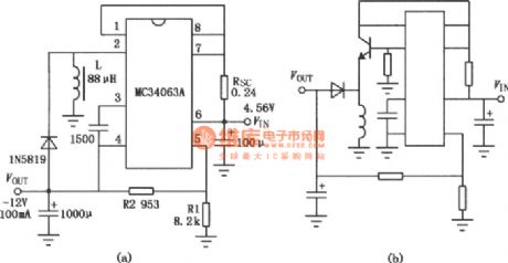
View full Circuit Diagram | Comments | Reading(853)
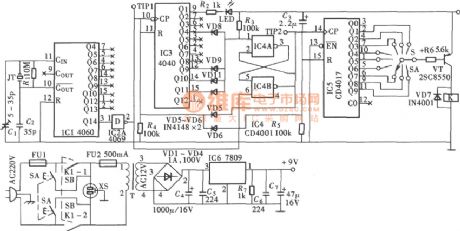
Automatic cycle timer circuit diagram
Published:2011/8/11 2:42:00 Author:Rebekka | Keyword: Automatic cycle timer
Automatic cycle timer circuit diagram is shown as above. It is composed of pulse oscillator, time base circuit composed of multi-level divider, double-contact state trigger, the relay, driver circuit and the power supply etc. (View)
View full Circuit Diagram | Comments | Reading(1462)
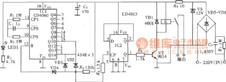
Precision adjustable timer(CD4017) circuit diagram
Published:2011/8/11 2:39:00 Author:Rebekka | Keyword: Precision adjustable timer
Precision adjustable timer(CD4017) circuit diagram is shown as above.
It uses crystal oscillator composed of CD4060 and quartz crystal to generate base signal. It is an adjustable timer using multi-level digital frequency circuit to make frequency division. (View)
View full Circuit Diagram | Comments | Reading(2282)
Any input voltage converting into 4 ~ 20mA V/ I converter circuit diagram
Published:2011/8/16 21:39:00 Author:Rebekka | Keyword: V/ I converter circuit , 4 ~ 20mA
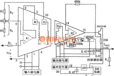
Any input voltage converting into 4 ~ 20mA V I converter circuit composed of isolated amplifier 3656 is shown as above.3656 amplifier is an isolated amplifier whichuses a hybrid integrated circuit for signal amplifier and isolation of power supply. It has a strong processing ability of analog signal because it uses an advanced modulation techniques and small hybrid transformer. The outstanding advantages of 3656 are: High adaptability and excellent performance. The ground terminals of input circuit, output circuit and power circuit are independentto each other. And they are not connected with each other to achieve the three-port isolation. (View)
View full Circuit Diagram | Comments | Reading(832)
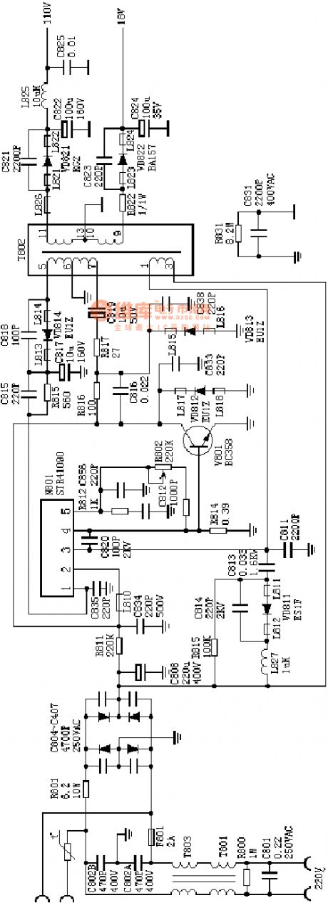
the absolutely useful switch power supply:the STR41090 power supply(A4)
Published:2011/8/13 6:46:00 Author:Ariel Wang | Keyword: absolutely useful , switch power supply
View full Circuit Diagram | Comments | Reading(743)
the absolutely useful switch power supply:the TDA two chips system power supply(A4)
Published:2011/8/13 6:49:00 Author:Ariel Wang | Keyword: absolutely useful , switch power supply, two chips system
View full Circuit Diagram | Comments | Reading(803)
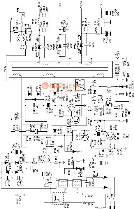
Beijing Cherokee Light Off-road Vehicle Fault Code Circuit
Published:2011/8/3 6:31:00 Author:Michel | Keyword: Beijing Cherokee, Fault Code Circuit
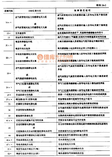
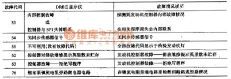
When the Cherokee light sport utility vehicle control circuit has a fault,the CHECKEN-GINE light on the dashboard will spark. The fault code which recorded by the computer will be displayed through manual or DRBII default indicator.In the 5 s,the ignition switch key turns again and again,which makes the ciruit become on-off-on-off-on and the fault code is displayed from the CHECKENGINE indicator.The light sparks for 3s and it is off (to test the bubble) and then the fault code is determined according to the flashing condition of lights and all codes indication are binary.There are 4s time interval among the codes.For example, the light flashes for four times and stops and then flashes for one time,which means that the fault code is 41. (View)
View full Circuit Diagram | Comments | Reading(747)
Record Microcomputer Running Time Counter Circuit of D51602
Published:2011/8/3 6:37:00 Author:Michel | Keyword: Running Time, Counter Circuit
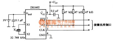
Picture 1 is record microcomputer running time counter circuit of D51602.This circuit is used to record microcomputer control running time.There are two 32-bit counter and the experienced time is counted in seconds.One is continuous work 32-bit counter and it counts the time of the microcomputer.The other is 32-bit counter of AC power supply and it counts the time of the microcomputer.Thus,we can know microcomputer work time and down time.
Picture 1:Record Microcomputer Running Time Counter Circuit of D51602
3 V battery and 32.768 kHz crystals Xl are added to DS1602 and it is connected to the microcomputer via the three thread and the circuit is very simple.32-bit counter can count for 136 years continously.Ac power is off , D51602 current consumption is less than 0.5 μA.And the battery life can be up to 10 years if 50 mAh capacity of the battery can be used.
(View)
View full Circuit Diagram | Comments | Reading(1036)
Measurement Standard Battery Benchmark Voltage Source Circuit of LM199
Published:2011/8/3 6:38:00 Author:Michel | Keyword: Standard Battery, Voltage Source Circuit

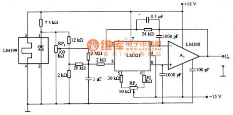
The picture is measurement standard battery benchmark voltage source circuit of LM199 and the benchmark source is 1.01V.The circuit consists of LM321 and LM308 etc. and disorders voltage is below 1μV/℃. The output voltage adjustment RP1 and temperature drift adjustable RP2 need to choose potentiometer with little temperature coefficient ,which does not affect the circuit. (View)
View full Circuit Diagram | Comments | Reading(834)
CXD254Q Digital Servo and Signal Processing Integrated Circuit
Published:2011/8/3 6:39:00 Author:Michel | Keyword: Digital Servo, Signal, Integrated Circuit
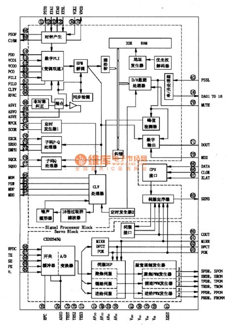
CXD254Q is digital servo and signal processing integrated circuit produced by Sony Company.It is widely used in CD and VCD players.
First,Inside Circuit Block DiagramCXD254Q integrated block circuitis mainly composed of digital servo(D-Servo) and signal processor (DSP).Its inside circuit block diagram is shown as picture 1.
Picture 1:Inside Circuit Block Diagram of CXD254Q Intergrated Block
(View)
View full Circuit Diagram | Comments | Reading(1595)
Thermistors Temperature or Frequency Conversion Circuit
Published:2011/8/1 0:27:00 Author:Michel | Keyword: Temperature, Frequency, Conversion Circuit
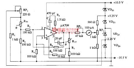
The picutre 3-6 is thermistor temperature or frequency conversion circuit.Because thermistors resistance changes with the temperature in linear way,the change can be used in voltage controlled oscillator.In the circuit,A1-A4 uses current type operational amplifier LM390O,RP1 and RP2 are used to adjust thermistors temperature-resistance properties and the voltage controlled oscillator voltage frequency characteristics.RP3 is used to regulate work range center of voltage controlled oscillator. Adjustment Process:When voltage controlled oscillator output voltage Ui is 7.5V and RP3are regulated,which makes output frequency f。 become 635Hz.lOkΩ calibrating resistance substitutes for thermistor RT and RP2 is regulated to make the output frequency f。 become 635Hz.Then 13·3kΩcalibrating resistance substitutes for thermistor RT again,RP1 is regulated to make the output frequency f。 become 143Hz.Please adjust like this for many times until the satisfying result is obtained. (View)
View full Circuit Diagram | Comments | Reading(805)
SM6781BV Charging Circuit
Published:2011/8/3 7:18:00 Author:Michel | Keyword: Charging Circuit
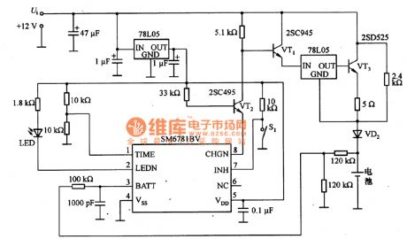
The above charging circuit is composed of SM6781BV.SM6781BV is charging control integrated controller and the tube feet functions are as follows.
Feet 1-Timing Choosing Port The value ofinput port voltage is set as UDD,UDD/2 or 0.
Feet 2(LEDN)-Charging Display LED Driving Output Port It adopts leakage output and the low PWL is output when it is fast charging.When the charging is abnormal and INH port is high PWL,the output pulse is 1HZ.And it is in high impedance condition when the charging is finished.
Feet 3(BATT)—Battery voltage Detection Input End This feet inputs every battery voltage and it adopts resistance to divide the voltage when there are many batteries.
Feet 7 (INH)—Fast Charging Interruptting Input Port It stops fast charging when it is high PWL.It stops charging and begins to charge when it is low PWL. (View)
View full Circuit Diagram | Comments | Reading(852)
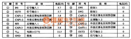
PT2380 Dolby Directional Logic Circuit and Tone Choice Intergrated Circuit
Published:2011/8/3 7:14:00 Author:Michel | Keyword: Dolby Directional, Logic Circuit, Tone Choice, Intergrated Circuit
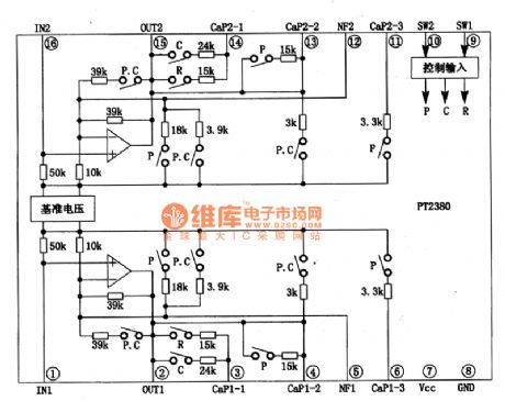
The input voltage of PT2380 is 100mV and work power voltage is 12V.Maximum output voltage undistortion is 3 V, noise level is 0.5-0.6 mV.There are 4 kinds of sound output mode in PT2380,namely,Normal/Flat (Flat), Rock,classical (pop) and POPS (communication).
The four tone modeis controlled by input PWL of SW1 and SW2(⑨ and ⑩ feet).Its inside circuit block diagram of intergrated block is shown as picture 1.
Picture 1:Inside Circuit Block Diagram of PT2380 Intergrated Circuit
Second,Pins Functions and DataPT2380 IC adopts 16 feet DIP package structure and its pins function and data are shown as table 1.
(View)
View full Circuit Diagram | Comments | Reading(1673)
Micropower Backup Power Supply Circuit of Voltage on Telephone Line
Published:2011/8/3 7:01:00 Author:Michel | Keyword: Telephone Line, Micropower, Backup, Power Supply Circuit
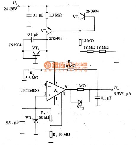
The micropower backup power supply circuit of voltage on telephone is as above.The input voltage Ui of micropower backup power supply absorbs from 24~28V telephone line and the input current is lower than 4μA.The output voltage U。of micropower backup power supply is 3.3V and the current is 1μA.In the circuit,VT1 and VT2 are current source and they provide about 3μA current for A1.A1 are reference voltage circuit and comparator circuit and the maximum static current consumption current is 0.6μA. (View)
View full Circuit Diagram | Comments | Reading(800)
S2560 Microcomputer Dailing Integrated Circuit
Published:2011/8/3 7:16:00 Author:Michel | Keyword: Microcomputer Dailing, Integrated Circuit
S2560 is the microcomputer dialing integrated circuit produced by American Microsoft Company and it is used in communication equipment and dialing integrated circuit.
S2560 integrated circuit can transfer keyboard input transformation into pulse signal output.It can also have storage telecommunication and suspending and redialing functions.It uses feet 18 DIP package structure and its pins functions and data are shown as table 1.
Table 1:S2560 IC Pins Functions and Data (View)
View full Circuit Diagram | Comments | Reading(545)
Southeast Ling Sheng light monitoring buzzer electric system circuit
Published:2011/8/6 21:39:00 Author:leo | Keyword: Light monitoring buzzer, electric system
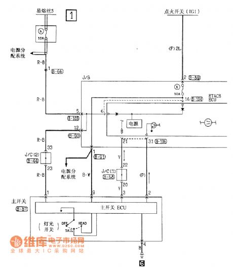
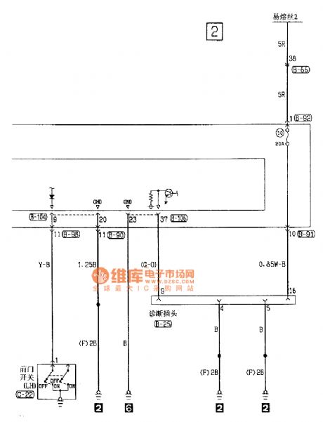
View full Circuit Diagram | Comments | Reading(774)
LOGIC_DRIVE_FOR_INDUCTIVE_LOAD
Published:2009/7/13 5:04:00 Author:May
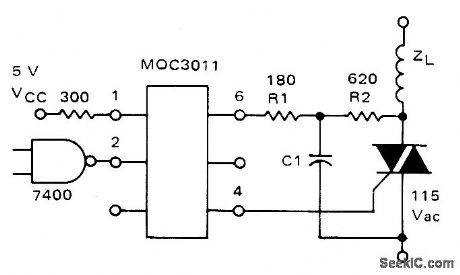
When output of NAND gate goes high and furnishes 10 mA to LED of Motorola M0C3011 optically coupled triac driver, output of optoisolator provides necessary trigger for triac controlling inductive load.C1 is 0.22 μF for load power factor of 0.75 and 0.33 μF for 0.5 power factor. Omit C1 for resistive load. R1, R2, and C1 serve as snubber that limits rate of rise in voltage applied to triac.-P. O'Neil, Applications of the MOC3011 Triac Driver, Motorola, Phoenix, AZ, 1978, AN-780 p 2. (View)
View full Circuit Diagram | Comments | Reading(1012)
| Pages:3/13 12345678910111213 |
Circuit Categories
power supply circuit
Amplifier Circuit
Basic Circuit
LED and Light Circuit
Sensor Circuit
Signal Processing
Electrical Equipment Circuit
Control Circuit
Remote Control Circuit
A/D-D/A Converter Circuit
Audio Circuit
Measuring and Test Circuit
Communication Circuit
Computer-Related Circuit
555 Circuit
Automotive Circuit
Repairing Circuit