
Other Circuit
Index 4
EXTERNAL_VOLTAGE_REFERENCE_WITH_BAR_GRAPH_DISPLAY_DRIVER
Published:2009/7/13 4:28:00 Author:May

Using external reference sources to produce (a) an adjustable 2 V and (b) up to +3V starting from +2 V. (View)
View full Circuit Diagram | Comments | Reading(684)
ON_OFF_INVERTERS
Published:2009/7/10 3:27:00 Author:May
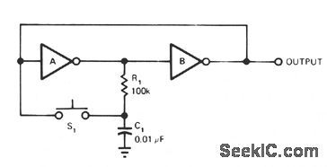
Each time the switch closes, the voltage on C1 causes inverter A to change state, with positive feedback from inverter B. Resistor R1 delays the charging and discharging of C1, making the circuit virtually immune to contact bounce. The circuit works with either CMOS or TTL gates. The values of R1 and C1 are not critical and can be increased for greater contact bounce protection, if needed.Recommended ranges are 10 K to 1 MΩ for R1, and 0.01 to 1.0 μF for C1. (View)
View full Circuit Diagram | Comments | Reading(675)
BIKE_SPEEDOMETER
Published:2009/7/10 2:18:00 Author:May
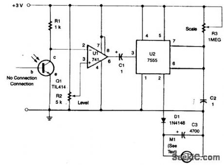
A TIL414 photo transistor senses reflection from a spoke-mounted reflector. This generates a pulse and sends it to U1 and U2, a monostable multi ibrator, which drives meter M1. (View)
View full Circuit Diagram | Comments | Reading(990)
GEIGER_COUNTER
Published:2009/7/20 0:45:00 Author:Jessie
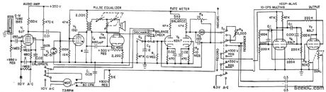
Simple basic monitor provides continuous audio end visual indications of radioactive materials in industrial areas. If recording is required, four leads at right are connected to 10-cps keep-alive mvbr and triode output stage for driving recorder. Will handle count rates up to 10,000 per minute. Strobotron V3 in pulse equalizer provides visual indications.-R. L. Ives, Geiger Radiation Monitor Indicates Continuously, Electronics, 31:43, p 93-95. (View)
View full Circuit Diagram | Comments | Reading(0)
Alternating_flasher_using_an_LM3909_chip
Published:2009/7/19 23:58:00 Author:Jessie
Alternating flasher using an LM3909 chip. Circuitry inside the dashes is the LM3909. This circuit is a relaxation oscillator flashing two LEDs sequentially. With a 12-volt DC supply the repetition rate is about 2.5 hertz (courtesy National Semiconductor Corporation). (View)
View full Circuit Diagram | Comments | Reading(739)
ELECTRONIC_ROULETTE_GAME
Published:2009/7/9 4:36:00 Author:May
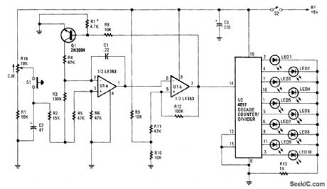
R14 is set for an initial starting speed of the oscillator U1A and U1B. As C2 charges, oscillation begins slowing down as C2 discharges, giving a roulette-wheel effect on LED S1 through 10. The LED that remains on is the winning number. (View)
View full Circuit Diagram | Comments | Reading(1504)
20_kHz_ARC_WELDING_INVERTER
Published:2009/7/8 23:33:00 Author:May
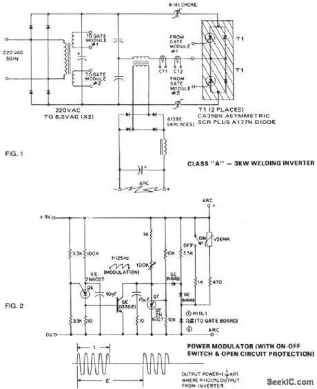
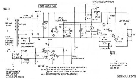
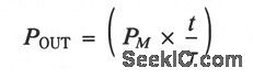
The Class A series resonant inverter portrayed is well-known and respected for its high efftciency, low cost, and small size, provided that operating frequency is greater than about 3 kHz. The disadvantages are, at least in high power versions, the difftculty in effecting smooth RFI-free output voltage modulationwithout significant added complexity, and a natural tendency to run away under no-load (highQ) conditions.The 20-kHz control circuit (see Fig. 2) overcomes these shortcomings by feeding back into the asymmetrical thyristor trigger pulse generators (see Fig. 3) signals that simultaneously shut the inverter down, when its output voltage exceeds a preset threshold, then time-ratio modulates the output. This feedback is accomplished with full galvanic isolation between input and output thanks to an H11L opto-Schmitt coupler. The fundamental 20-kHz gate firing pulses are generated by a PUT relaxation oscillator Q1. The pulses are then amplified by transistors Q2 and Q3. The 20-kHz sinusoidal load current flowing in the pri-mary of the output transformer is then detected by current transformer CT1, with op amp A1 converting the sine wave into a square wave, whose transitions coincide with the load current zero points.Consequently, each time the output current changes, phase A1 also changes state and, via transistor Q4, either connects the thyristor gate to a -8 Vdc supply for minimum gate assisted turn-off time and highest reapplied dVldt capability or disables this supply to prepare the thyristor for subsequent firing.Modulation intelligence is coupled into this same H11L through two additional PUTs, Q6 and Q7, Q6 oscillates at a fixed 1.25 kHz, which establishes the modulation frequency. The duty cycle is determined by a second oscillator, Q7, whose conduction state, on or off, establishes or removes current from the H11L diode. With afundamental inverter frequency of 20 kHz and a modulation frequency of 1.25 kHz, the resultant time ratio-controlled power output is given by:where PM= 100% continuous output power. Minimum power is one cycle of 20 kHz (50 μs) in the 1.25-kHz modulation frame (800 μs), that is, 6.25% PM. (View)
View full Circuit Diagram | Comments | Reading(5097)
ULTRASONIC_PEST_REPELLER
Published:2009/7/8 23:28:00 Author:May
This circuit is a 555 timer IC connected as a square-wave generator. Its base frequency is approximately 45 kHz, as determined by the values of R1, R2, and C1. The 45-kHz carrier is frequency modulated by a modified trapizoidal voltage waveform applied to pin 5 of the 555 timer. That modulating voltage is developed by a network consisting of C2, R3, and R4 connected across one leg of the bridge rectifier. The sweep is approximately 20 kHz on each side of the base frequency. The speaker is a 2-inch piezoelectric tweeter. (View)
View full Circuit Diagram | Comments | Reading(0)
2__37_V
Published:2009/7/8 23:27:00 Author:May
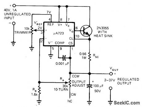
Simple circuit glves fine linear controlwith 10-turn pot over wide voltage range by first using 10K trimmer pot to divide 7-V reference down to 2 V.-G. Dressel, Regulator Circuit Provides Linear 2-37 V Adjustment Range, EDNMagazine, March 5, 1978, p 122. (View)
View full Circuit Diagram | Comments | Reading(871)
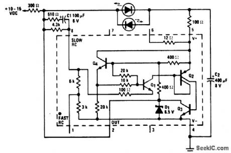
±15V_AT_200_mA
Published:2009/7/8 23:26:00 Author:May
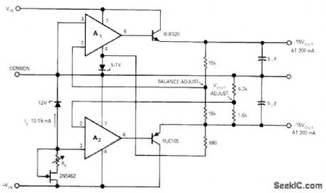
Two-opamp regulatorgives dual-polarity tracking outputs that can be balanced to within millivolts of each other or can be offset as required. Negative voltage is regulated, and positive output tracks negative. Article gives step-by-step design procedure based on use of pA741 or equivalent opamps. AC ripple is less than 2 mV P-P. Conventional full-wave bridge rectifier with capacitor-input filter can be used to provide rectuired unregulated 36 VDC for inputs.-C. Brogado, IC Op Amps Simplify Regulator Design, E.DNlEEEMagazine, Jan.15, 1972, p 30-34. (View)
View full Circuit Diagram | Comments | Reading(713)
0_15_MHz_WITH_100_dB_CMR_
Published:2009/7/8 5:35:00 Author:May
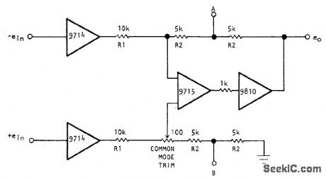
Differential inputs are applied to Optical Electronics 9715 opamp through 9714 voltage followers. Currentbooster using 9810 opamp raises load current to ±100 mA. Complete amplifier has very high differential and common-mode input impedance. Common-mode rejection can be trimmed to greater than 100 dB at 1 kHz for unity gain.Gain is determined by value of resistor RG connected between points A and B and is equal to(2R2/R1)(1 + 2R2/RG). Settling time is 500 ns.Accuracy is maintained from -550C to +85 0C-''Instrumentation Ampliffer, Optical Electronics, Tucson, AZ, Application Tip 10240. (View)
View full Circuit Diagram | Comments | Reading(698)
TEMPERATURE_TRANSDUCER_INTERFACE
Published:2009/7/8 5:17:00 Author:May
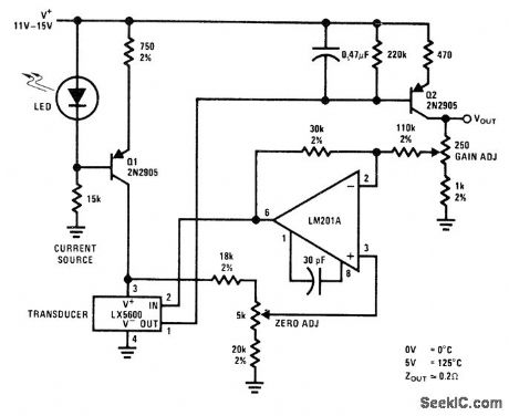
Output of National LX5600 temperature-sensing transducer is inverted, level-shifted, and given extra voltage gain of 4 to give required output of0 to +5 V for telemetry system or instrumentation recorder. Q1 furnishes constant current to thermometer, and Q2 provides inverting function. Resulting output signal is reinverted by LM201A opamp connected through zero-adjust divider to pin 3 which provides voltage reference.-P. Lefferts, A New Interfacing Concept; the Monolithic Temperature Transducer, National Semiconductor, Santa Clara, CA, 1975, AN-132, p 3. (View)
View full Circuit Diagram | Comments | Reading(611)
_SPEED_CONTEOLLED_REVERSIBLE_DC_MOTOR_VRIVE
Published:2009/7/8 5:12:00 Author:May
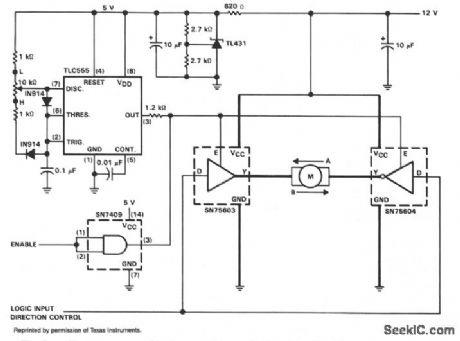
The figure illustrates a reversible dc motor drive application with adjustable speed control. The D inputs for these drivers are complementary and can be tied together and driven from the same logic control for bidirectional motor drive. The enables are tied together and driven by a pulse-width-modulated generator providing on duty cycles of 10 to 90% for speed control. A separate enable control is provided through an SN7409 logic gate. See the truth table for this motor controller application.
Definitions for the terms used in the truth table are as follows:
EN EnableDC Direction controlSP.C Speed controlA Direction of current-right to leftB Direction of current-left to rightH Logic 1 voltage levelL Logic 0 voltage levelN Speed control set for narrow pulse width Speed control set for wide pulse widthX Irrelevant (View)
View full Circuit Diagram | Comments | Reading(1910)
APPROXIMATING_COSINES
Published:2009/7/7 22:34:00 Author:May
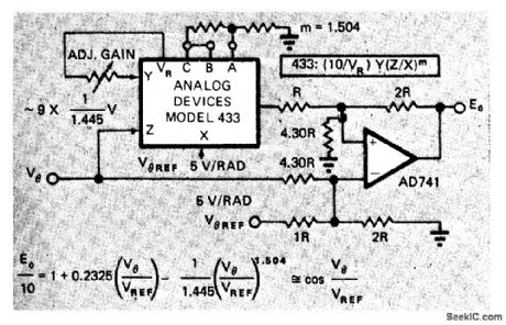
Analog Devices 433 multiplier/divider IC approximates cosine of angle to better than 1%, by computing nonintegral exponents. 0nly one opamp is needed. Approximation uses arbitrary exponent as one term of cosineθplus a linear term and a constant term, as described in article.-D. H. Sheingold, Approximate Analog Functions with a Low-Cost Multiplier/Divider, EDN Magazine, Feb. 5, 1973, p 50-52. (View)
View full Circuit Diagram | Comments | Reading(639)
DICE
Published:2009/7/7 22:16:00 Author:May
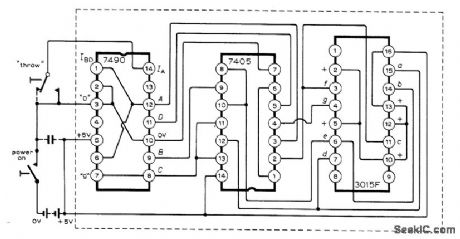
Simple low-cost arrangement of three ICs operating from 5-V battery (four nickel-cadmium or alkaline cells) provides bar display corresponding to spots on six sides of die. Uses SN7490N TTL decade counter with SN7405 hex inverter to drive Minitron 3015F seven-segment display. Article describes operation in detail and suggests variations for Arabic and binary displays.-G,J,Naaijer,Electronic Dice,Wireless World,Aug 1973,p401-403. (View)
View full Circuit Diagram | Comments | Reading(1725)
HOCKEY_TENNIS_HANDBALL
Published:2009/7/7 21:34:00 Author:May
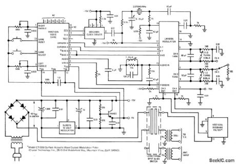
Uses National have sound. MM57100 TV game chip to provide logic for generatingbackgrounds, paddles, ball, and dig ital scoring Circuit generates all necessary timing (sync, blanking, and burst) to interface with interface directly to antenna terminals of set.-MM57100 TV game chip to provide Iogic for ing (sync, blanking, and burst) to interface with circuit of standard TV receiver. With addition ofchroma, audio, and RF modulator, circuit will interface directly to antenna terminals of set.-''MOS/LSI Databook, National Semiconductor,Santa Clara, CA, 1977, p 4-37-4-47. (View)
View full Circuit Diagram | Comments | Reading(816)
ELECTRONIC_DICE
Published:2009/7/7 7:00:00 Author:May
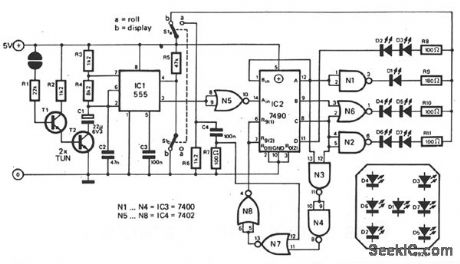
The basic die circuit is given. A 555 timer, IC1, is connected as an astable multivibrator. This feeds clock pulses to divide-by-six counter IC2 the outputs of which are decoded by gates N1 to N6 to drive an array of LEDs in the familiar die pattern. When switch S1 is in position b, the reset input of IC1 decreases and the oscillator is inhibited. Power is fed to the LEDs via Slb so that the display is activated. When the die is rolled 'oy switching 51 to position a, the display is blanked. C4 is connected to positive supply via Sla, producing a short pulse which resets IC2 via N7 and N8. The reset input of IC1 is pulled high via R5, so the multivibrator begins to oscillate and feeds clock pulses to IC2 via NS. When S1 is switched back to position a, the multivibrator is again inhibited. Then, the counter stops and power is applied to the LEDs which display the value of the throw. (View)
View full Circuit Diagram | Comments | Reading(0)
Setting Timing Circuit of Power Supply Connection
Published:2011/7/26 0:54:00 Author:Michel | Keyword: Power Supply, Setting Timing Circuit
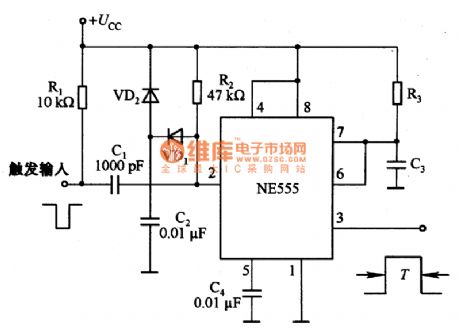
Picture 1 is setting timing circuit of power supply connection.When the power is connected,triggering PWL of ME555 feet 2 is below (1/3)Ucc and feet 3 outputs pulse during the time decided by R2 and C2.Then,+Ucc charges C2 via R2 and VD1 and charging voltage rises to +Ucc.Because of VD1 isolation function,R1 and C1 negative trigger the pulse.VD1 is fast charging diode when the power is off and it can keep the circuit working reliably when the circuit is off and turned on again and again in short time.NE55 outputs T high-level of pulse which is determined by R3 and C3,namely, T=R3C3.
Picture 1:Setting Timing Circuit of Power Supply Connection (View)
View full Circuit Diagram | Comments | Reading(673)
Monolithic Stereo Play Intergrted Circuit
Published:2011/7/20 2:06:00 Author:Michel | Keyword: Monolithic, Stereo, Play Intergrted Circuit
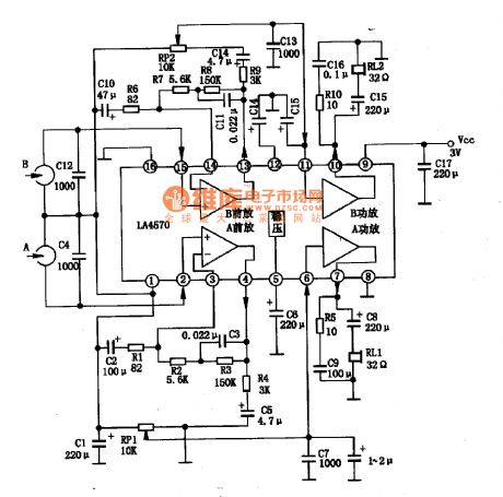
LA4570 is cassette specific integrated circuit produced by SANYO Company.LA4570 are used in domestic, domestic assembly or import the monoplayer and cassette player.
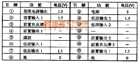
First,LA4570 Inside Circuit Block Diagram and Pins FunctionsLA4570 integrated block is double preamplifying double power amplifier devices, with low voltage power supply and wide range, high gain, low consumption and less external components etc.advantages.One LA4570 and few external device can constitute monoplayer and cassette player.Its intergrated block inside circuit block diagram and typical application circuit are shown as picture 1.The IC adopts 16 feet DIP or flat package structure. The IC pins functions and data are shown as table 1.
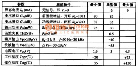
Table 1: LA4570 IC Pins Functions and DataLA4570 Typical Application Circuit LA4570 typical application circuit of intergrated block is shown as picture 1. (View)
View full Circuit Diagram | Comments | Reading(1897)
TLC2932 Phase Locked Loop Clock Generating Integrated Circuit
Published:2011/7/20 1:34:00 Author:Michel | Keyword: Phase Locked, Loop Clock, Generating Integrated Circuit
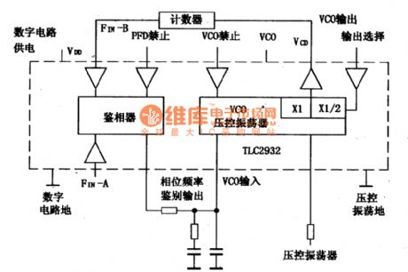
TLC2932 is FLL clock generating IC produced by TEXAS.TLC2932 is mostly used in the DLP projection TV, in order to provide the clock signal for processing
circuits.TLC2932 integrated circuit contains the analog vco and phase detection circuit.Its inside circuit block diagram of intergrated block is shown as picture 1-1.
Picture 1-1:Inside Circuit Block Diagram of TLC2932 Intergrated Block
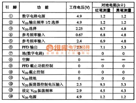
TL2932 adopts 14 feet DIP package and its pins functions and data are shown as table 1-2.
Table 1-2:Pins Functions and Data ofTLC2932 IC
(View)
View full Circuit Diagram | Comments | Reading(933)
| Pages:4/13 12345678910111213 |
Circuit Categories
power supply circuit
Amplifier Circuit
Basic Circuit
LED and Light Circuit
Sensor Circuit
Signal Processing
Electrical Equipment Circuit
Control Circuit
Remote Control Circuit
A/D-D/A Converter Circuit
Audio Circuit
Measuring and Test Circuit
Communication Circuit
Computer-Related Circuit
555 Circuit
Automotive Circuit
Repairing Circuit