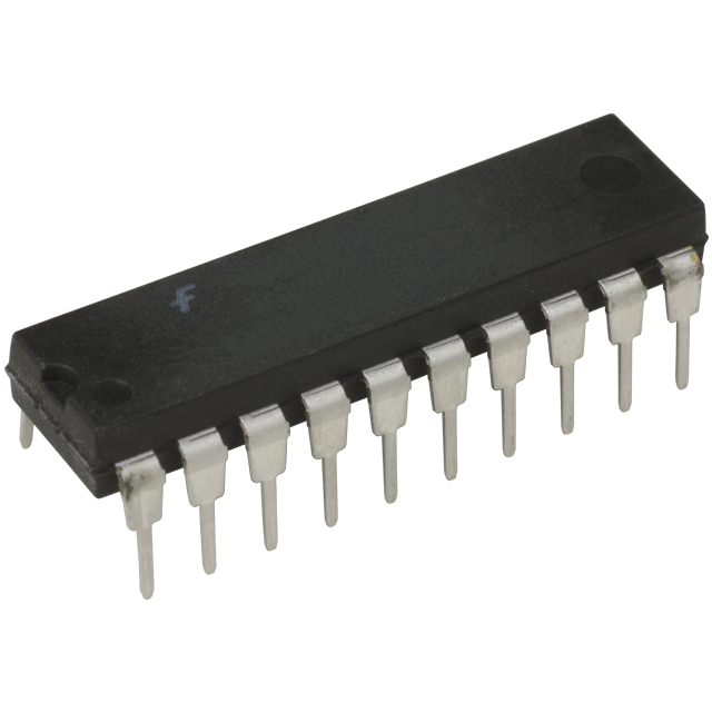
Want to post a buying lead? If you are not a member yet, please select the specific/related part number first and then fill the quantity and your contact details in the "Request for Quotation Form" on the left, and then click "Send RFQ".Your buying lead can then be posted, and the reliable suppliers will quote via our online message system or other channels soon.
The AC273 and ACT273 have eight edge-triggered D-type flip-flops with individual D-type inputs and Q outputs. The common buffered Clock (CP) and Master Reset (MR) input load and reset (clear) all flip-flops simultaneously.
The register is fully edge-triggered. The state of each Dtype input, one setup time before the LOW-to-HIGH clock transition, is transferred to the corresponding flip-flop's Q output.
All outputs will be forced LOW independently of Clock or Data inputs by a LOW voltage level on the MR input. The device is useful for applications where the true output only is required and the Clock and Master Reset are common to all storage elements.
74AC273PC Maximum Ratings
Supply Voltage (VCC).................. −0.5V to +7.0V DC Input Diode Current (IIK) VI = −0.5V ......................................... −20 mA VI = VCC + 0.5V................................. +20 mA DC Input Voltage (VI) .........−0.5V to VCC + 0.5V DC Output Diode Current (IOK) VO = −0.5V........................................ −20 mA VO = VCC + 0.5V +20 mA DC Output Voltage (VO) ......−0.5V to VCC + 0.5V DC Output Source or Sink Current (IO)............................ ±50 mA DC VCC or Ground Current per Output Pin (ICC or IGND)............... ±50 mA Storage Temperature (TSTG)... −65°C to +150°C Junction Temperature (TJ) PDIP ......................................................140°C
74AC273PC Features
Ideal buffer for microprocessor or memory Eight edge-triggered D-type flip-flops Buffered common clock Buffered, asynchronous master reset See 377 for clock enable version See 373 for transparent latch version See 374 for 3-STATE version Outputs source/sink 24 mA 74ACT273 has TTL-compatible inputs
74AC273PC Connection Diagram
74AC273SC Parameters
Technical/Catalog Information
74AC273SC
Vendor
Fairchild Semiconductor
Category
Integrated Circuits (ICs)
Mounting Type
Surface Mount
Package / Case
20-SOIC
Function
Master Reset
Number of Bits per Element
8
Number of Elements
1 - Single
Current - Output High, Low
24mA, 24mA
Output Type
Non-Inverted
Trigger Type
Positive Edge
Type
D-Type Bus
Packaging
Tube
Operating Temperature
-40°C ~ 85°C
Delay Time - Propagation
5.5ns
Frequency - Clock
175MHz
Voltage - Supply
2 V ~ 6 V
Lead Free Status
Lead Free
RoHS Status
RoHS Compliant
Other Names
74AC273SC 74AC273SC
74AC273SC General Description
The AC273 and ACT273 have eight edge-triggered D-type flip-flops with individual D-type inputs and Q outputs. The common buffered Clock (CP) and Master Reset (MR) input load and reset (clear) all flip-flops simultaneously.
The register is fully edge-triggered. The state of each Dtype input, one setup time before the LOW-to-HIGH clock transition, is transferred to the corresponding flip-flop's Q output.
All outputs will be forced LOW independently of Clock or Data inputs by a LOW voltage level on the MR input. The device is useful for applications where the true output only is required and the Clock and Master Reset are common to all storage elements.
74AC273SC Maximum Ratings
Supply Voltage (VCC).................. −0.5V to +7.0V DC Input Diode Current (IIK) VI = −0.5V ......................................... −20 mA VI = VCC + 0.5V................................. +20 mA DC Input Voltage (VI) .........−0.5V to VCC + 0.5V DC Output Diode Current (IOK) VO = −0.5V........................................ −20 mA VO = VCC + 0.5V +20 mA DC Output Voltage (VO) ......−0.5V to VCC + 0.5V DC Output Source or Sink Current (IO)............................ ±50 mA DC VCC or Ground Current per Output Pin (ICC or IGND)............... ±50 mA Storage Temperature (TSTG)... −65°C to +150°C Junction Temperature (TJ) PDIP ......................................................140°C
74AC273SC Features
Ideal buffer for microprocessor or memory Eight edge-triggered D-type flip-flops Buffered common clock Buffered, asynchronous master reset See 377 for clock enable version See 373 for transparent latch version See 374 for 3-STATE version Outputs source/sink 24 mA 74ACT273 has TTL-compatible inputs