Want to post a buying lead? If you are not a member yet, please select the specific/related part number first and then fill the quantity and your contact details in the "Request for Quotation Form" on the left, and then click "Send RFQ".Your buying lead can then be posted, and the reliable suppliers will quote via our online message system or other channels soon.
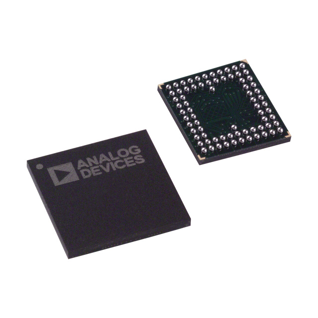
The AD5516 is a 16-channel, 12-bit voltage-output DAC. The selected DAC register is written to via the 3-wire serial interface.DAC selection is accomplished via address bits A3A0. 14-bit resolution can be achieved by fine adjustment in Increment/ Decrement Mode (Mode 2). The serial interface operates at clock rates up to 20 MHz and is compatible with standard SPI, MICROWIRE, and DSP interface standards. The output voltage range is fixed at ±2.5 V (AD5516-1), ±5 V (AD5516-2),and ±10 V (AD5516-3). Access to the feedback resistor in each channel is provided via RFB 0 to R FB 15 pins.
The device is operated with AV CC= 5 V ± 5%, DV CC= 2.7 V to 5.25 V, VSS = 4.75 V to 12 V, and VDD = +4.75 V to +12 V and requires a stable 3 V reference on REF_IN.
AD5516ABC-1 Maximum Ratings
(TA= 25°C unless otherwise noted.) VDDto AGND . . . . . . . . . . . . . . . . . . . . . . . . . . . . . 0.3 V to +17 V VSSto AGND . . . . . . . . . . . . . . . . . . . . . . . . . .. . . .+0.3 V to 17 V AVCC to AGND, DACGND . . . . . . . . . . . . . . . . . . . . .0.3 V to +7 V DVCC to DGND . . . . . . . . . . . . . . . . . . . . . . . . . . . . .0.3 V to +7 V Digital Inputs to DGND . . . . . . . . . . . . . . . . 0.3 V to DVCC +0.3 V Digital Outputs to DGND . . . . . . . . . . . . . . . 0.3 V to DVCC +0.3 V REF_IN to AGND, DACGND . . . . . . . . . . . . . .0.3 V to AVCC+ 0.3 V VOUT 015 to AGND . . . . . . . . . . . . . . . VSS 0.3 V to VDD +0.3 V AGND to DGND . . . . . . . . . . . . . . . . . . . . . . . . . .. 0.3 V to +0.3 V RFB015 to AGND . . . . . . . . . . . . . . . . . . VSS 0.3 V to VDD+0.3 V Operating Temperature Range, Industrial . . . .. .40°C to +85°C Storage Temperature Range . . . . . . . . . . . . . . .65°C to +150°C Junction Temperature (TJMAX) . . . . . . . . . . . . . .. . . . . . . . . .150°C 74-Lead LFBGA Package, Thermal Impedance . .. . . . . . . . 41°C/W Reflow Soldering Peak Temperature . . . . . . . . . . . . . . . . . . . . . . . . . . . . . . . .220°C Time at Peak Temperature . . . . . . . . . . . . . . . . . .10 sec to 40 sec
AD5516ABC-1 Features
High Integration: 16-Channel DAC in 12 mm 14-Bit Resolution via Increment/Decrement Mode Guaranteed Monotonic Low Power, SPITM, QSPITM, MICROWIRETM,and DSPCompatible 3-Wire Serial Interface Output Impedance 0.5 Output Voltage Range ±2.5AD5516-1 ±5 V (AD5516-2) ±10 V (AD5516-3) Asynchronous Reset-Facility (via RESET Pin) Asynchronous Power-Down Facility (via PD Pin) Daisy-Chain Mode Temperature Range: 40 to + 85
APPLICATIONS Level Setting Instrumentation Automatic Test Equipment Optical Networks Industrial Control Systems Data Acquisition Low Cost I/O
AD5516ABC-1 Typical Application
The AD5516 is suited for use in many applications, such as levelsetting, optical, industrial systems, and automatic test applications. In level setting and servo applications where a fine-tune adjust is required, the Mode 2 function increases resolution.The following figures show the AD5516 used in some potential applications.