Want to post a buying lead? If you are not a member yet, please select the specific/related part number first and then fill the quantity and your contact details in the "Request for Quotation Form" on the left, and then click "Send RFQ".Your buying lead can then be posted, and the reliable suppliers will quote via our online message system or other channels soon.
The AD9876 is a single-supply broadband modem mixed-signal front end (MxFE) IC. The device contains a transmit path interpolation filter and DAC and a receive path PGA, LPF, and ADC supporting a variety of broadband modem applications.Also on-chip is a PLL clock multiplier that provides all required clocks from a single crystal or clock input. The AD9876 provides 12-bit converter performance on both the Tx and Rx path.
The TxDAC+ uses a selectable digital 2* or 4* interpolation low-pass or band-pass filter to further oversample transmit data and reduce the complexity of analog reconstruction filtering. The transmit path signal bandwidth can be as high as 26 MHz at an input data rate of 64 MSPS. The 12-bit DAC provides differential current outputs for optimum noise and distortion performance. The DAC full-scale current can be adjusted from 2 to 20 mA by a single resistor, providing 20dB of additional gain range.
The receive path consists of a PGA, LPF, and ADC. The PGA has a gain range of 6 dB to +36 dB, programmable in 2 dB steps, adding 42 dB of dynamic range to the receive path. The path LPF cutoff frequency can be programmed to either 12 MHz or 26 MHz. The filter cutoff frequency can also be tuned or bypassed where filter requirements differ. The 12-bit ADC uses a multistage differential pipeline architecture to achieve excellent dynamic performance with low power consumption.
The AD9876 provides a voltage regulator controller (VRC) that can be used with an external power MOSFET transistor to form a cost-effective 1.3 V linear regulator. The digital transmit and receive ports are each multiplexed to a bus width of six bits and are clocked at a frequency of twice the 12-bit word rate. The AD9876 ADC and/or DAC can also be used at sampling rates as high as 64 MSPS in a 6-bit resolution nonmulti-plexed mode.
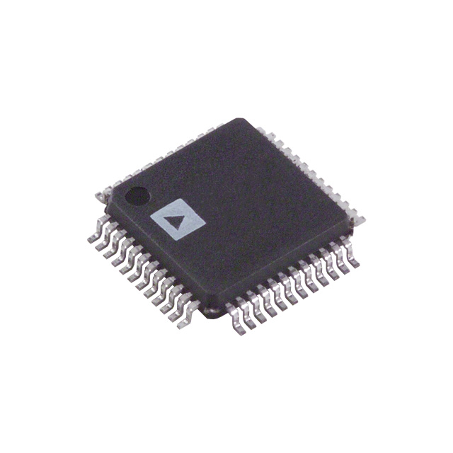
The AD9876 is pin compatible with the 10-bit AD9875. Both are available in a space-saving 48-lead LQFP package. They are speci- fied over the industrial (40°C to +85°C) temperature range.receive
AD9876 Maximum Ratings
Power Supply (VS) . . . . . . . . . . . . . . . . . . . . . . . . . . 3.9 V Digital Output Current . . . . . . . . . . . . . . . . . . . . . . .5 mA Digital Inputs . . . . . . . . . . . . . .0.3 V to DRVDD + 0.3 V Analog Inputs . . . . . . . . . . . . . . 0.3 V to AVDD + 0.3 V Operating Temperature . . . . . . . . . . .40°C to +85°C Maximum Junction Temperature . . . . . . . . . . . . . 150°C Storage Temperature . . . . . . . . . . . .65°C to +150°C Lead Temperature (Soldering 10 sec) . . . . . . . . .300°C
AD9876 Features
Low Cost 3.3 V CMOS Mixed-Signal Front End (MxFE(TM)) Converter for Broadband Modems 10-/12-Bit D/A Converter (TxDAC+ (R)) 64/32 MSPS Input Word Rate 2 /4 Interpolating LPF or BPF Transmit Filter 128 MSPS DAC Output Update Rate Wide (26 MHz) Transmit Bandwidth Power-Down Mode 10-/12-Bit 50 MSPS A/D Converter Fourth Order Low-Pass Filter 12 MHz or 26 MHz with Bypass 6 dB to +36 dB Programmable Gain Amplifier Internal Clock Multiplier (PLL) Clock Outputs Voltage Regulator Controller 48-Lead LQFP Package
AD9876 Typical Application
Powerline Networking Home Phone Networking xDSL Broadband Wireless Home RF