Want to post a buying lead? If you are not a member yet, please select the specific/related part number first and then fill the quantity and your contact details in the "Request for Quotation Form" on the left, and then click "Send RFQ".Your buying lead can then be posted, and the reliable suppliers will quote via our online message system or other channels soon.
The ADL5330 is a high performance, voltage-controlled variable gain amplifier/attenuator for use in applications with frequencies up to 3 GHz. The balanced structure of the signal path minimizes distortion while it also reduces the risk of spurious feed-forward at low gains and high frequencies caused by parasitic coupling. While operation between a balanced source and load is recommended, a single-sided input is internally converted to differential form.
The input impedance is 50 from INHI to INLO. The outputs are usually coupled into a 50 grounded load via a 1:1 balun. A single supply of 4.75 V to 5.25 V is required.
The 50 input system converts the applied voltage to a pair of differential currents with high linearity and good common rejection even when driven by a single-sided source. The signal currents are then applied to a proprietary voltage-controlled attenuator providing precise definition of the overall gain under the control of the linear-in-dB interface. The GAIN pin accepts a voltage from 0 V at minimum gain to 1.4 V at full gain with a 20 mV/dB scaling factor.
The output of the high accuracy wideband attenuator is applied to a differential transimpedance output stage. The output stage sets the 50 differential output impedances and drives Pin OPHI and Pin OPLO. The ADL5330 has a power-down function. It can be powered down by a Logic LO input on the ENBL pin. The current consumption in power-down mode is 250 A.
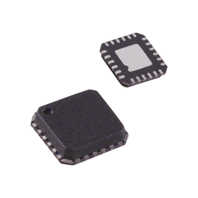
The ADL5330 is fabricated on an ADI proprietary high performance, complementary bipolar IC process. The ADL5330 is available in a 24-lead (4 mm * 4 mm), Pb-free LFCSP_VQ package and is specified for operation from ambient temperatures of −40°C to +85°C. An evaluation board is also available.
ADL5330 Maximum Ratings
Parameter
Rating
Supply Voltage VPS1, VPS2 RF Input Power at Maximum Gain OPHI, OPLO ENBL GAIN Internal Power Dissipation JA (with Pad Soldered to Board) Maximum Junction Temperature Operating Temperature Range Storage Temperature Range Lead Temperature Range (Soldering 60 sec)
5.5 V 5 dBm at 50 5.5 V VPS1, VPS2 2.5 V 1.1 W 60°C/W 150°C −40°C to +85°C −65°C to +150°C 300°C
ADL5330 Features
Voltage-controlled amplifier/attenuator Operating frequency 10 MHz to 3 GHz Optimized for controlling output power High linearity: OIP3 31 dBm @ 900 MHz Output noise floor: −150 dBm/Hz @ 900 MHz 50 input and output impedances Single-ended or differential operation Wide gain-control range: −34 dB to +22 dB @ 900 MHz Linear-in-dB gain control function, 20 mV/dB Single-supply 4.75 V to 5.25 V