Want to post a buying lead? If you are not a member yet, please select the specific/related part number first and then fill the quantity and your contact details in the "Request for Quotation Form" on the left, and then click "Send RFQ".Your buying lead can then be posted, and the reliable suppliers will quote via our online message system or other channels soon.
The ADM1177 is an integrated hot swap controller that offers digital current and voltage monitoring via an on-chip, 12-bit analog-to-digital converter (ADC), communicated through an I2C interface.
An internal current sense amplifier senses voltage across the sense resistor in the power path via the VCC pin and the SENSE pin.
The ADM1177 limits the current through this resistor by control-ling the gate voltage of an external N-channel FET in the power path, via the GATE pin. The sense voltage (and, therefore, the inrush current) is kept below a preset maximum.
The ADM1177 protects the external FET by limiting the time that it spends with maximum current running through it. This current limit period is set by the choice of capacitor attached to the TIMER pin. Additionally, the device provides protection from overcurrent events that may occur once the hot swap event is complete. In the case of a short-circuit event, the current in the sense resistor exceeds an overcurrent trip threshold, and the FET is switched off immediately by pulling down the GATE pin.
A soft start (SS) pin is also included. This gives the user control over the reference on the current sense amplifier. An internal current source charges a capacitor on this pin at startup, allowing the user to set the profile of the initial current ramp. A voltage can also be driven on this pin to alter the reference.
A 12-bit ADC can measure the current seen in the sense resistor, as well as the supply voltage on the VCC pin. An industry-standard I2C interface allows a controller to read current and voltage data from the ADC. Measurements can be initiated by an I2C command. Alternatively, the ADC can run continuously, and the user can read the latest conversion data whenever it is required. Up to four unique I2C addresses can be created, depending on the way the ADR pin is connected.
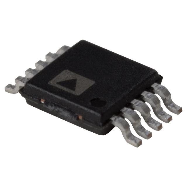
The ADM1177 is packaged in a 10-lead MSOP.
ADM1177 Maximum Ratings
Parameter
Rating
VCC Pin
20 V
SENSE Pin
20 V
TIMER Pin
−0.3 V to +6 V
ON Pin
−0.3 V to +20 V
SS Pin
−0.3 V to +6 V
GATE Pin
30 V
SDA Pin, SCL Pin
−0.3 V to +7 V
ADR Pin
−0.3 V to +6 V
Storage Temperature Range
−65°C to +125°C
Operating Temperature Range
−40°C to +85°C
Lead Temperature Range (Soldering, 10 sec)
300°C
Junction Temperature
150°C
Stresses above those listed under Absolute Maximum Ratings may cause permanent damage to the device. This is a stress rating only; functional operation of the device at these or any other conditions above those indicated in the operational section of this specification is not implied. Exposure to absolute maximum rating conditions for extended periods may affect device reliability.
ADM1177 Features
·Allows safe board insertion and removal from a live backplane ·Controls supply voltages from 3.15 V to 16.5 V ·Precision current sense amplifier ·Precision voltage input ·12-bit ADC for current and voltage readback ·Charge pumped gate drive for external N-channel FET ·Adjustable analog current limit with circuit breaker ·±3% accurate hot swap current limit level ·Fast response limits peak fault current ·Automatic retry or latch-off on current fault ·Programmable hot swap timing via TIMER pin ·Soft start pin for reference adjustment and programming of initial current ramp rate ·Active-high ON pin ·I2C® fast mode-compliant interface (400 kHz maximum) ·10-lead MSOP
ADM1177 Typical Application
·Power monitoring/power budgeting ·Central office equipment ·Telecommunication and data communication equipment ·PCs/servers