Want to post a buying lead? If you are not a member yet, please select the specific/related part number first and then fill the quantity and your contact details in the "Request for Quotation Form" on the left, and then click "Send RFQ".Your buying lead can then be posted, and the reliable suppliers will quote via our online message system or other channels soon.
DDTA143ZCA 7 F DDTA143ZCA7F DDTA143ZCA FDIDKR ND DDTA143ZCAFDIDKRND DDTA143ZCA-FDIDKR
DDTA144ECA Maximum Ratings
Part Number
DDTA144ECA
Product Type
PNP
Max Output Current ICM (mA)
-100
Max PD (mW)
200
Bias Resistors R1 (KW)
47
Bias Resistors R2 (KW)
47
DDTA144ECA-7-02 General Description
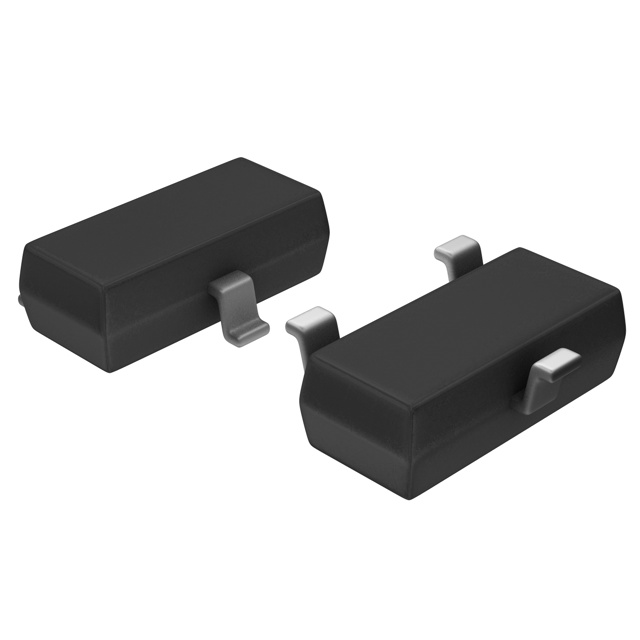
DDTA144ECA-7-02 is one type of DDTA144ECA-7-F. The following is some information about the DDTA144ECA-7-F. It is a kind of PNP pre-biased small signal surface mount transistor. It is available in SOT-23 package. There are some features as follows. (1)epitaxial planar die construction; (2)complementary NPN types available (DDTC); (3)built-in biasing resistors, R1 = R2; (4)lead free/RoHS compliant.
What comes next is about the maximum ratings (TA = 25 unless otherwise specified). (1):VCC (Supply Voltage) is -50 V; (2):VIN (Input Voltage) is from +10 to -40 V; (3):IO (Output Current) is -30 mA; (4):IC (Output Current, All) is -100 mA; (4): Pd (Power Dissipation) is 200 mW; (5): RJA (Thermal Resistance, Junction to Ambient Air) is 625/W; (6):Tj, Tstg (Operating and Storage Temperature) is from -55 to 150.
The following is about the electrical characteristics (TA = 25 unless otherwise specified). (1): the minimum VI(off) (input voltage) is -0.5 V and the typical is -1.1 V at VCC=5 V, IO=100A; (2):the typical VI(on) (input voltage) is -1.9 V and the maximum is -3 V at VCC=0.3 V, IO=2 mA; (3):the typical VO(on) (output voltage) is -0.1 V and the maximum is -0.3 V at IO/Il=10 mA/0.5 mA.