L4991, L4991TM1, L4992 Selling Leads, Datasheet
MFG:NS Package Cooled:QFN-8 D/C:NSC


MFG:NS Package Cooled:QFN-8 D/C:NSC

Want to post a buying lead? If you are not a member yet, please select the specific/related part number first and then fill the quantity and your contact details in the "Request for Quotation Form" on the left, and then click "Send RFQ".Your buying lead can then be posted, and the reliable suppliers will quote via our online message system or other channels soon.
TOP
PDF/DataSheet Download
Datasheet: L4901
File Size: 137029 KB
Manufacturer: STMICROELECTRONICS [STMicroelectronics]
Download : Click here to Download
PDF/DataSheet Download
Datasheet: L4901
File Size: 137029 KB
Manufacturer: STMICROELECTRONICS [STMicroelectronics]
Download : Click here to Download
PDF/DataSheet Download
Datasheet: L4992
File Size: 315649 KB
Manufacturer: STMicro
Download : Click here to Download
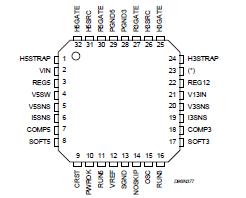
The L4992 is a sophisticated dual PWM stepdown controller and power monitor intended for Notebook computer and/or battery powered equipment. The device produces regulated +3.3V, +5.1V and 12V supplies for use in portable and PCMCIA applications.
The internal architecture allows to operate with minimum external components count. A very high switching frequency (200/300 KHz or externally synchronizable) optimizes their physical dimensions.
Synchronous rectification and pulse skipping mode for the buck sections optimise the overall efficiency over a wide load current range (96% efficiency @1A/5.1V and 93% efficiency @ 0.05A/5.1V.
The two high performance PWM controllers for +3.3V and +5.1V lines are monitored for overvoltage, undervoltage and overcurrent conditions. On detection of a fault, a POWER GOOD signal is generated and a specific shutdown procedure takes place to prevent physical damage and data corruption.
A disable function allows to manage the output power sections separately, optimising the quiescent consumption of the IC in stand-by conditions.
| Symbol | Parameter |
Value |
Unit |
| VIN | Power Supply Voltage on VIN |
0 to 25 |
V |
| VI | Maximum Pin Voltage to Pins 1, 24, 25, 32 |
-0.5 to (VIN +5) |
V |
| IIN | Input Current Except V13IN and VIN |
-1 to +1 |
mA |
| IOUT | Output Current Digital Output |
-15 to +15 |
mA |
| TJ | junction temperature |
-55 to +150 |

Price: 4-6 USD
MT58L64L18CT-10 TQFP100

Price: 5-6.5 USD
DL-7140-211M laser tube

Price: 4-5 USD
74LVC74APG - IC FLIP FLOP D-Type POS-EDG DUAL 14TSSOP

Price: 6.5-8 USD
CYPRESS - Clock Synthesizer with Differential CPU Outputs

Price: 0.284-0.286 USD
PI5V330QEX Pericom Multiplexer Switch ICs

Price: 1-2 USD
IGBT power module, Single switch, 1200 V, Collector-emitter voltage, 430A

Price: 1-2 USD
a-Si TFT-LCD, NEC, 228.096Hmm, 560V

Price: 0.124-0.2 USD
PC354N1T - Mini-flat Package, AC Input Type Photocoupler - Sharp Electrionic Components

Price: 0.177-0.178 USD
RL1210JR51-XX-BL - Thick Film Chip Resistor Low Ohmic - TAITRON Components Incorporated

Price: 0.053-0.055 USD
STPS140A - POWER SCHOTTKY RECTIFIER - STMicroelectronics

Price: 1.45-1.5 USD
STA013 - MPEG 2.5 LAYER III AUDIO DECODER - STMicroelectronics

Price: 0.073-0.075 USD
SMBJ5347B - 5 Watt Surface Mount Silicon Zener Diodes - Micro Commercial Components

