LMP7716MMX, LMP7717, LMP7731 Selling Leads, Datasheet
MFG:NSC Package Cooled:N/A D/C:08+

LMP7716MMX, LMP7717, LMP7731 Datasheet download

Part Number: LMP7716MMX
MFG: NSC
Package Cooled: N/A
D/C: 08+


MFG:NSC Package Cooled:N/A D/C:08+
LMP7716MMX, LMP7717, LMP7731 Datasheet download
MFG: NSC
Package Cooled: N/A
D/C: 08+

Want to post a buying lead? If you are not a member yet, please select the specific/related part number first and then fill the quantity and your contact details in the "Request for Quotation Form" on the left, and then click "Send RFQ".Your buying lead can then be posted, and the reliable suppliers will quote via our online message system or other channels soon.
TOP
PDF/DataSheet Download
Datasheet: LMP2011
File Size: 705032 KB
Manufacturer: NSC [National Semiconductor]
Download : Click here to Download
PDF/DataSheet Download
Datasheet: LMP2011
File Size: 705032 KB
Manufacturer: NSC [National Semiconductor]
Download : Click here to Download
PDF/DataSheet Download
Datasheet: LMP2011
File Size: 705032 KB
Manufacturer: NSC [National Semiconductor]
Download : Click here to Download
The LMP7717 (single) and the LMP7718 (dual) low noise, CMOS input operational amplifiers offer a low input voltage noise density of 5.8 nV/Hz while consuming only 1.15 mA (LMP7717) of quiescent current. The LMP7717/LMP7718 are stable at a gain of 10 and have a gain bandwidth (GBW) product of 88 MHz. The LMP7717/LMP7718 have a supply voltage range of 1.8V to 5.5V and can operate from a single supply. The LMP7717/LMP7718 each feature a rail-to-rail output stage. Both amplifiers are part of the LMP® precision amplifier family and are ideal for a variety of instrumentation applications.
The LMP7717 family provides optimal performance in low voltage and low noise systems. A CMOS input stage, with typical input bias currents in the range of a few femto-Amperes, and an input common mode voltage range, which includes ground, make the LMP7717/LMP7718 ideal for low power sensor applications where high speeds are needed.
The LMP7717/LMP7718 are manufactured using National's advanced VIP50 process. The LMP7717 is offered in either a 5-Pin SOT23 or an 8-Pin SOIC package. The LMP7718 is offered in either the 8-Pin SOIC or the 8-Pin MSOP.
ESD Tolerance (Note 2)
Human Body Model ..................2000V
Machine Model .....................200V
VIN Differential ....................±0.3V
Supply Voltage (V+ V−) ...............6.0V
Input/Output Pin Voltage V+........+0.3V, V− −0.3V
Storage Temperature Range....... −65°C to 150°C
Junction Temperature (Note 3) ...........+150°C
Soldering Information
Infrared or Convection (20 sec) ...........235°C
Wave Soldering Lead Temp (10 sec).........260°C
Operating Ratings (Note 1)
Temperature Range (Note 3)....... −40°C to 125°C
Supply Voltage (V+ V−)
−40°C TA 125°C .............2.0V to 5.5V
0°C TA 125°C............... 1.8V to 5.5V
Package Thermal Resistance (JA (Note 3))
5-Pin SOT23 ....................180°C/W
8-Pin SOIC .....................190°C/W
8-Pin MSOP .................. ..236°C/W

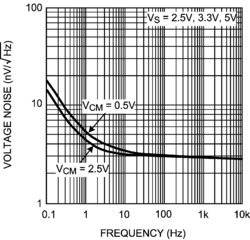
The LMP7731 is a single, low noise, rail-to-rail input and output, low voltage amplifier. The LMP7731 is part of the LMP precision amplifier family and is ideal for precision and low noise applications with low voltage requirements.
This operational amplifier offers low voltage noise of 2.9 nV/
The LMP7731 provides a wide GBW of 22 MHz while consuming only 2 mA of current. This high gain bandwidth along with the high open loop gain of 130 dB enables accurate signal conditioning in applications with high closed loop gain requirements.
The LMP7731 has a supply voltage range of 1.8V to 5.5V, making it an ideal choice for battery operated portable applications.
The LMP7731 is offered in the space saving 5-Pin SOT-23 and 8-Pin SOIC packages.
Design Tools
| Title | Size in Kbytes | Date | |||
| WEBENCH Sensor Designer Tool | View |
If you have trouble printing or viewing PDF file(s), see Printing Problems. |
Application Notes
| Title | Size in Kbytes | Date | |
| AN-1873: Application Note 1873 DC Parameters | 249 Kbytes | 19-Jun-08 | Download |
| AN-1873 (Chinese): Application Note 1873 DC Parameters | 379 Kbytes | ||
| AN-1515: Application Note 1515 A Comprehensive Study of the Howland Current Pump | 227 Kbytes | 29-Jan-08 | Download |
If you have trouble printing or viewing PDF file(s), see Printing Problems. |
| Offset Voltage max, 25C | 0.05 mV |
| TcVos | 1 uV/degC |
| CMRR | 120 dB |
| PSRR | 129 dB |
| Avol | 130 dB |
| Voltage Noise | 2.9 nV/root(Hz) |
| Max Input Bias Current | 85 nA |
| Gain Bandwidth | 22 MHz |
| Supply Current Per Channel | 2.2 mA |
| PowerWise Rating 2 | 100 uA/MHz |
| Slew Rate | 2.4 Volts/usec |
| Channels | 1 Channels |
| Supply Min | 2.5 Volt |
| Supply Max | 5 Volt |
| Input OutputType | R-R In and Out |
| Output Current | 47 mA |
| Shut down | No |
| Special Features | Ultra Low Noise |
| Temperature Min | -40 deg C |
| Temperature Max | 125 deg C |
| Function | Op Amp |
| Automotive Selection Guide | Yes |
| PowerWise | Yes |
| View Using Catalog | |

Price: 4-6 USD
MT58L64L18CT-10 TQFP100

Price: 5-6.5 USD
DL-7140-211M laser tube

Price: 4-5 USD
74LVC74APG - IC FLIP FLOP D-Type POS-EDG DUAL 14TSSOP

Price: 6.5-8 USD
CYPRESS - Clock Synthesizer with Differential CPU Outputs

Price: 0.284-0.286 USD
PI5V330QEX Pericom Multiplexer Switch ICs

Price: 1-2 USD
IGBT power module, Single switch, 1200 V, Collector-emitter voltage, 430A

Price: 1-2 USD
a-Si TFT-LCD, NEC, 228.096Hmm, 560V

Price: 0.124-0.2 USD
PC354N1T - Mini-flat Package, AC Input Type Photocoupler - Sharp Electrionic Components

Price: 0.177-0.178 USD
RL1210JR51-XX-BL - Thick Film Chip Resistor Low Ohmic - TAITRON Components Incorporated

Price: 0.053-0.055 USD
STPS140A - POWER SCHOTTKY RECTIFIER - STMicroelectronics

Price: 1.45-1.5 USD
STA013 - MPEG 2.5 LAYER III AUDIO DECODER - STMicroelectronics

Price: 0.073-0.075 USD
SMBJ5347B - 5 Watt Surface Mount Silicon Zener Diodes - Micro Commercial Components
