M74HCT367M1R, M74HCT373R13TR, M74HCT374 Selling Leads, Datasheet
MFG:ST Package Cooled:09+ D/C:1000

M74HCT367M1R, M74HCT373R13TR, M74HCT374 Datasheet download

Part Number: M74HCT367M1R
MFG: ST
Package Cooled: 09+
D/C: 1000


MFG:ST Package Cooled:09+ D/C:1000
M74HCT367M1R, M74HCT373R13TR, M74HCT374 Datasheet download
MFG: ST
Package Cooled: 09+
D/C: 1000

Want to post a buying lead? If you are not a member yet, please select the specific/related part number first and then fill the quantity and your contact details in the "Request for Quotation Form" on the left, and then click "Send RFQ".Your buying lead can then be posted, and the reliable suppliers will quote via our online message system or other channels soon.
TOP
PDF/DataSheet Download
Datasheet: M74HCT367M1R
File Size: 253989 KB
Manufacturer: STMICROELECTRONICS [STMicroelectronics]
Download : Click here to Download
PDF/DataSheet Download
Datasheet: M74AC574B
File Size: 83392 KB
Manufacturer: STMICROELECTRONICS [STMicroelectronics]
Download : Click here to Download
PDF/DataSheet Download
Datasheet: M74HCT374
File Size: 146656 KB
Manufacturer: ST
Download : Click here to Download
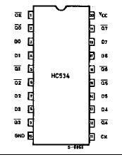
The M54/74HCT374, M54/74HCT534, are high speed CMOS OCTAL D-TYPE FLIPFLOP WITH 3- STATE OUTPUTS fabricated with in silicon gate C2MOS technology. They have the same high speed performance of LSTTL combined with true CMOS low power comsuption. These8-bit D-type flip-flops are controlled by a clock input (CK) and an ouput enable input (OE). On the positive transition of the clock, the Q outputs will be set to the logic state that were setup at the D inputs (HCT374) or their complements (HCT534).
While the OE input is low, the eight outputs will be in a normal logic state (high or low logic level), and while high level, the outputs will be in a high impedance state. The output control does not affect the internal operation of flip-flops. That is, the old data can be retained or the new data can be entered even while the outputs are off. The application engineer has a choice of combination of inverting and non-inverting outputs. The 3-state output configuration and the wide choice of outline make bus-organized systems simple. All inputs are equipped with protection circuits against static discharge and transient excess voltage. This integrated circuit has input and output characteristics that are fully compatible with 54/74 LSTTL logic families. M54/74HCT devices are designed to directly interface HSC2MOS systems with TTL and NMOS components. They are also plug in replacements for LSTTL devices giving a reduction of power consumption.
|
Symbol |
Parameter |
Value |
Unit |
|
VCC |
Supply Voltage |
-0.5 to +7 |
V |
|
VI |
DC Input Voltage |
-0.5 to VCC + 0.5 |
V |
|
VO |
DC Output Voltage |
-0.5 to VCC + 0.5 |
V |
|
IIK |
DC Input Diode Current |
± 20 |
mA |
|
IOK |
DC Output Diode Current |
± 20 |
mA |
|
IO |
DC Output Source Sink Current Per Output Pin |
± 35 |
mA |
|
ICC or IGND |
DC VCC or Ground Current |
± 70 |
mA |
|
PD |
Power Dissipation |
500 (*) |
mW |
|
Tstg |
Storage Temperature |
-65 to +150 |
°C |
|
TL |
Lead Temperature (10 sec) |
300 |
°C |

Price: 4-6 USD
MT58L64L18CT-10 TQFP100

Price: 5-6.5 USD
DL-7140-211M laser tube

Price: 4-5 USD
74LVC74APG - IC FLIP FLOP D-Type POS-EDG DUAL 14TSSOP

Price: 6.5-8 USD
CYPRESS - Clock Synthesizer with Differential CPU Outputs

Price: 0.284-0.286 USD
PI5V330QEX Pericom Multiplexer Switch ICs

Price: 1-2 USD
IGBT power module, Single switch, 1200 V, Collector-emitter voltage, 430A

Price: 1-2 USD
a-Si TFT-LCD, NEC, 228.096Hmm, 560V

Price: 0.124-0.2 USD
PC354N1T - Mini-flat Package, AC Input Type Photocoupler - Sharp Electrionic Components

Price: 0.177-0.178 USD
RL1210JR51-XX-BL - Thick Film Chip Resistor Low Ohmic - TAITRON Components Incorporated

Price: 0.053-0.055 USD
STPS140A - POWER SCHOTTKY RECTIFIER - STMicroelectronics

Price: 1.45-1.5 USD
STA013 - MPEG 2.5 LAYER III AUDIO DECODER - STMicroelectronics

Price: 0.073-0.075 USD
SMBJ5347B - 5 Watt Surface Mount Silicon Zener Diodes - Micro Commercial Components
