Want to post a buying lead? If you are not a member yet, please select the specific/related part number first and then fill the quantity and your contact details in the "Request for Quotation Form" on the left, and then click "Send RFQ".Your buying lead can then be posted, and the reliable suppliers will quote via our online message system or other channels soon.
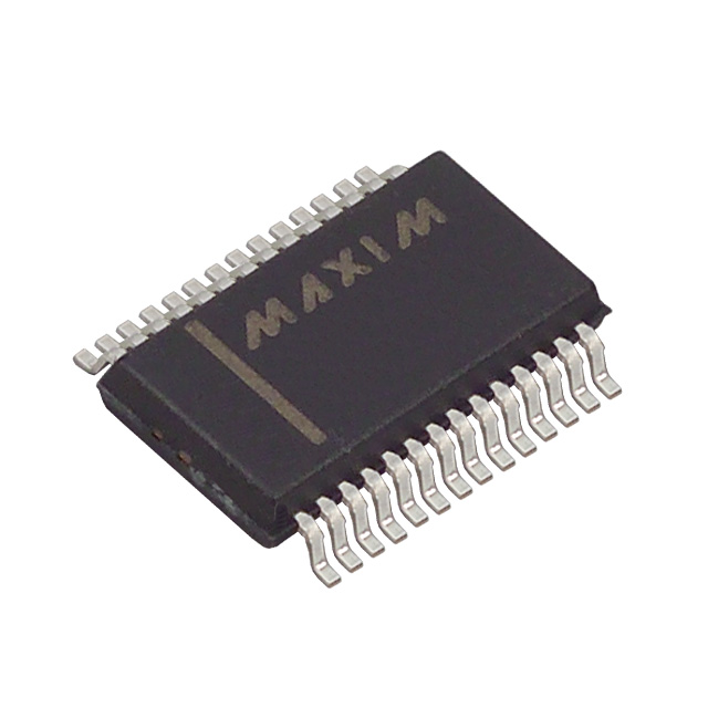
The MAX1290/MAX1292 low-power,12-bit analog-to-digital converters (ADCs) feature a successive-approxi-mation ADC, automatic power-down, fast wake-up (2µs), an on-chip clock, +2.5V internal reference, and a high-speed, byte-wide parallel interface. The devices operate with a single +5V analog supply and feature a VLOGIC pin that allows them to interface directly with a +2.7V to +5.5V digital supply.Power consumption is only 10mW (VDD= VLOGIC) at a 400ksps max sampling rate. Two software-selectable power-down modes enable the MAX1290/MAX1292 to be shut down between conversions; accessing the par-allel interface returns them to normal operation.Powering down between conversions can cut supply current to under 10µA at reduced sampling rates. Both devices offer software-configurable analog inputs for unipolar/bipolar and single-ended/pseudo-differen-tial operation. In single-ended mode, the MAX1290 has eight input channels and the MAX1292 has four input channels (four and two input channels, respectively,when in pseudo-differential mode).Excellent dynamic performance and low power, com-bined with ease of use and small package size, make these converters ideal for battery-powered and data-acquisition applications or for other circuits with demand-ing power consumption and space requirements. The MAX1290/MAX1292 tri-states INT when CS goes high. Refer to MAX1262/MAX1264 if tri-stating INT is not desired.The MAX1290 is available in a 28-pin QSOP package,while the MAX1292 comes in a 24-pin QSOP. For pin-compatible +3V, 12-bit versions, refer to the MAX1291/MAX1293 data sheet.
MAX1290 Maximum Ratings
VDDto GND..............................................................-0.3V to +6V VLOGICto GND.........................................................-0.3V to +6V CH0CH7, COM to GND............................-0.3V to (VDD+ 0.3V) REF, REFADJ to GND.................................-0.3V to (VDD+ 0.3V) Digital Inputs to GND...............................................-0.3V to +6V Digital Outputs (D0D11, INT ) to GND...........................................-0.3V to (VLOGIC+ 0.3V) Continuous Power Dissipation (TA= +70°C) 24-Pin QSOP (derate 9.5mW/°C above +70°C).........762mW 28-Pin QSOP (derate 8.00mW/°C above +70°C).......667mW Operating Temperature Ranges MAX1290_C_ _/MAX1292_C_ _.......................0°C to +70°C MAX1290_E_ _/MAX1292_E_ _.....................-40°C to +85°C Storage Temperature Range.............................-65°C to +150°C Lead Temperature (soldering, 10s).................................+300°C