Want to post a buying lead? If you are not a member yet, please select the specific/related part number first and then fill the quantity and your contact details in the "Request for Quotation Form" on the left, and then click "Send RFQ".Your buying lead can then be posted, and the reliable suppliers will quote via our online message system or other channels soon.
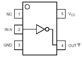
The NL17SV04 is an ultra-high performance inverter manufactured in 0.35 m technology, with excellent performance down to 0.9 V.
This device is ideal for extremely high speed and high-drive applications. Additionally, limitations of board space are no longer a constraint. The very small SOT?553 makes this device fit most tight designs and spaces.
NL17SV04XV5T2 Maximum Ratings
Symbol
Parameter
Value
Unit
VCC
DC Supply Voltage
−0.5 to + 4.6
V
VIN
DC Input Voltage
−0.5 to + 4.6
V
VOUT
DC Output Voltage
−0.5 to VCC +0.5
V
IIK
DC Input Diode Current VI < GND
±50
mA
IOK
DC Output Diode Current VO = GND VO = VCC
−50 +50
mA
IOU
DC Output Sink Current
±50
mA
ICC
DC Supply Current per Supply Pin
±50
mA
IGND
DC Ground Current per Ground Pin
±50
mA
TSTG
Storage Temperature Range
−65 to +150
°C
TL
Lead Temperature, 1 mm from Case for 10 Seconds
260
°C
TJ
Junction Temperature Under Bias
+150
°C
JA
Power Dissipation in Still Air at 85°C
250
°C/W
PD
Power Dissipation in Still Air at 85°C
250
mW
MSL
Moisture Sensitivity
Level 1
FR
Flammability Rating Oxygen Index: 28 to 34
UL 94 V−0 @ 0.125 in
VESD
ESD Withstand Voltage Human Body Model (Note 2) Machine Model (Note 3)
4000 150
V
Maximum ratings are those values beyond which device damage can occur. Maximum ratings applied to the device are individual stress limit values (not normal operating conditions) and are not valid simultaneously. If these limits are exceeded, device functional operation is not implied, damage may occur and reliability may be affected. 1.Measured with minimum pad spacing on an FR4 board, using 10 mm-by-1 inch, 2 ounce copper trace no air flow. 2.Tested to EIA/JESD22-A114-A. 3.Tested to EIA/JESD22-A115-A.
NL17SV04XV5T2 Features
· Extremely High Speed: t PD = 1.0 ns (Typ) @ V CC = 3.3 V · Designed for 0.9 to 3.6 V Operation · Overvoltage Tolerance (OVT)* Input Pins Permits Logic Translation · Balanced 24 mA Output Drive @ VCC 3.3 Volts · Near Zero Static Supply Current · Ultra-Tiny SOT-553 5 Pin Package only 1.6 x 1.6 x 0.6 mm · All Devices in Package SOT-553 are Inherently Pb-Free**