RF2413, RF2415TR13, RF2416 Selling Leads, Datasheet
MFG:RF Package Cooled:SOP D/C:97+

RF2413, RF2415TR13, RF2416 Datasheet download

Part Number: RF2413
MFG: RF
Package Cooled: SOP
D/C: 97+


MFG:RF Package Cooled:SOP D/C:97+
RF2413, RF2415TR13, RF2416 Datasheet download
MFG: RF
Package Cooled: SOP
D/C: 97+

Want to post a buying lead? If you are not a member yet, please select the specific/related part number first and then fill the quantity and your contact details in the "Request for Quotation Form" on the left, and then click "Send RFQ".Your buying lead can then be posted, and the reliable suppliers will quote via our online message system or other channels soon.
TOP
PDF/DataSheet Download
Datasheet: RF2413
File Size: 190301 KB
Manufacturer: RFMD [RF Micro Devices]
Download : Click here to Download
PDF/DataSheet Download
Datasheet: RF2
File Size: 756593 KB
Manufacturer: Willow Technologies Ltd
Download : Click here to Download
PDF/DataSheet Download
Datasheet: RF2416
File Size: 427640 KB
Manufacturer: RFMD [RF Micro Devices]
Download : Click here to Download
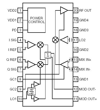
The RF2413 is a monolithic integrated transmitter universal modulation IC capable of generating modulated AM, PM, or compound carriers in the VHF/UHF frequency range. The modulation is performed at VHF, then the resulting spectrum is upconverted to a frequency range between 100MHz and 1000MHz. Up to 60dB of power control is possible through the use of two gain control pins. The IC contains all of the required components to implement the modulation function including differential amplifiers for the baseband inputs, a 90° hybrid phase splitter, limiting LO amplifiers, two balanced mixers, a combining, gain-controlled differential amplifier, a second balanced mixer, and an output gain-controlled RF amplifier which will drive a 50Ω load.
| Parameter |
Rating |
Unit |
| Supply Voltage Input LO and RF Levels I and Q Modulation Levels Operating Ambient Temperature Storage Temperature |
-0.5 to 7.0 +6 VDD -40 to +85 -40 to +150 |
VDC dBm V °C °C |
The RF2416 is a dual-band low noise amplifier with bypass switch designed for use as a front-end for 950MHz GSM and DCS1800/PCS1900 applications. It may also be used for dual-band cellular/PCS application. The 900MHz LNA is a single-stage amplifier with bypass switch; the 1800/1900 LNA is a two-stage amplifier with bypass switch. Both amplifiers have excellent noise figure and high linearity in both high gain and bypass/low gain mode. The device is packaged in a 3mmx3mm, 12 pin, leadless chip carrier.
| Parameter |
Rating |
Unit |
| Supply Voltage Input RF Level Storage Temperature |
-0.5 to +6.0 +10 -40 to +150 |
VDC dBm °C |


Price: 4-6 USD
MT58L64L18CT-10 TQFP100

Price: 5-6.5 USD
DL-7140-211M laser tube

Price: 4-5 USD
74LVC74APG - IC FLIP FLOP D-Type POS-EDG DUAL 14TSSOP

Price: 6.5-8 USD
CYPRESS - Clock Synthesizer with Differential CPU Outputs

Price: 0.284-0.286 USD
PI5V330QEX Pericom Multiplexer Switch ICs

Price: 1-2 USD
IGBT power module, Single switch, 1200 V, Collector-emitter voltage, 430A

Price: 1-2 USD
a-Si TFT-LCD, NEC, 228.096Hmm, 560V

Price: 0.124-0.2 USD
PC354N1T - Mini-flat Package, AC Input Type Photocoupler - Sharp Electrionic Components

Price: 0.177-0.178 USD
RL1210JR51-XX-BL - Thick Film Chip Resistor Low Ohmic - TAITRON Components Incorporated

Price: 0.053-0.055 USD
STPS140A - POWER SCHOTTKY RECTIFIER - STMicroelectronics

Price: 1.45-1.5 USD
STA013 - MPEG 2.5 LAYER III AUDIO DECODER - STMicroelectronics

Price: 0.073-0.075 USD
SMBJ5347B - 5 Watt Surface Mount Silicon Zener Diodes - Micro Commercial Components
