Want to post a buying lead? If you are not a member yet, please select the specific/related part number first and then fill the quantity and your contact details in the "Request for Quotation Form" on the left, and then click "Send RFQ".Your buying lead can then be posted, and the reliable suppliers will quote via our online message system or other channels soon.
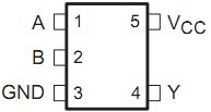
The SN74AHC1G86 is a single 2-input exclusive-OR gate. The device performs the Boolean function Y = A B or Y = AB + AB in positive logic.
A common application is as a true/complement element. If one of the inputs is low, the other input is reproduced in true form at the output. If one of the inputs is high, the signal on the other input is reproduced inverted at the output.
SN74AHC1G86DCKT Maximum Ratings
Supply voltage range, VCC . . . . . . . . . . . . . . . . . . . . . . . . . . . . . . −0.5 V to 7 V Input voltage range, VI (see Note 1) . . . . . . . . . . . . . . . . . . . . . .−0.5 V to 7 V Output voltage range, VO (see Note 1) . . . . . . . . . . . . . −0.5 V to VCC + 0.5 V Input clamp current, IIK (VI < 0) . . . . . . . . . . . . . . . . . . . . . . . . . . . . . .−20 mA Output clamp current, IOK (VO < 0 or VO > VCC) . . . . . . . . . . . . . . . . . .±20 mA Continuous output current, IO (VO = 0 to VCC) . . . . . . . . . . . . . . . . . . .±25 mA Continuous current through VCC or GND . . . . . . . . . . . . . . . . . . . . . . . .±50 mA Package thermal impedance, JA (see Note 2): DBV package . . . . . .206°C/W DCK package . . . . . .252°C/W DRL package . . . . . .142°C/W Storage temperature range, Tstg . . . . . . . . . . . . . . . . . . . . . . .−65°C to 150°C † Stresses beyond those listed under "absolute maximum ratings" may cause permanent damage to the device. These are stress ratings only, and functional operation of the device at these or any other conditions beyond those indicated under "recommended operating conditions" is not implied. Exposure to absolute-maximum-rated conditions for extended periods may affect device reliability. NOTES: 1. The input and output voltage ratings may be exceeded if the input and output current ratings are observed. 2. The package thermal impedance is calculated in accordance with JESD 51-7.
SN74AHC1G86DCKT Features
Operating Range of 2 V to 5.5 V Max tpd of 8 ns at 5 V Low Power Consumption, 10-µA Max ICC ±8-mA Output Drive at 5 V Schmitt Trigger Action at All Inputs Makes the Circuit Tolerant for Slower Input Rise and Fall Time Latch-Up Performance Exceeds 250 mA Per JESD 17 ESD Protection Exceeds JESD 22 − 2000-V Human-Body Model (A114-A) − 200-V Machine Model (A115-A) − 1000-V Charged-Device Model (C101)
The SN74AHC1G86 is a single 2-input exclusive-OR gate. The device performs the Boolean function Y = A B or Y = AB + AB in positive logic.
A common application is as a true/complement element. If one of the inputs is low, the other input is reproduced in true form at the output. If one of the inputs is high, the signal on the other input is reproduced inverted at the output.
SN74AHC1G86DRLR Maximum Ratings
Supply voltage range, VCC . . . . . . . . . . . . . . . . . . . . . . . . . . . . . . −0.5 V to 7 V Input voltage range, VI (see Note 1) . . . . . . . . . . . . . . . . . . . . . .−0.5 V to 7 V Output voltage range, VO (see Note 1) . . . . . . . . . . . . . −0.5 V to VCC + 0.5 V Input clamp current, IIK (VI < 0) . . . . . . . . . . . . . . . . . . . . . . . . . . . . . .−20 mA Output clamp current, IOK (VO < 0 or VO > VCC) . . . . . . . . . . . . . . . . . .±20 mA Continuous output current, IO (VO = 0 to VCC) . . . . . . . . . . . . . . . . . . .±25 mA Continuous current through VCC or GND . . . . . . . . . . . . . . . . . . . . . . . .±50 mA Package thermal impedance, JA (see Note 2): DBV package . . . . . .206°C/W DCK package . . . . . .252°C/W DRL package . . . . . .142°C/W Storage temperature range, Tstg . . . . . . . . . . . . . . . . . . . . . . .−65°C to 150°C † Stresses beyond those listed under "absolute maximum ratings" may cause permanent damage to the device. These are stress ratings only, and functional operation of the device at these or any other conditions beyond those indicated under "recommended operating conditions" is not implied. Exposure to absolute-maximum-rated conditions for extended periods may affect device reliability. NOTES: 1. The input and output voltage ratings may be exceeded if the input and output current ratings are observed. 2. The package thermal impedance is calculated in accordance with JESD 51-7.
SN74AHC1G86DRLR Features
Operating Range of 2 V to 5.5 V Max tpd of 8 ns at 5 V Low Power Consumption, 10-µA Max ICC ±8-mA Output Drive at 5 V Schmitt Trigger Action at All Inputs Makes the Circuit Tolerant for Slower Input Rise and Fall Time Latch-Up Performance Exceeds 250 mA Per JESD 17 ESD Protection Exceeds JESD 22 − 2000-V Human-Body Model (A114-A) − 200-V Machine Model (A115-A) − 1000-V Charged-Device Model (C101)