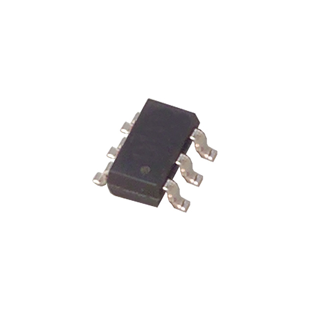
Want to post a buying lead? If you are not a member yet, please select the specific/related part number first and then fill the quantity and your contact details in the "Request for Quotation Form" on the left, and then click "Send RFQ".Your buying lead can then be posted, and the reliable suppliers will quote via our online message system or other channels soon.
This single Schmitt-trigger buffer is designed for 1.65-V to 5.5-V VCC operation.
The SN74LVC1G17 contains one buffer and performs the Boolean function Y = A. The device functions as an independent buffer, but because of Schmitt action, it may have different input threshold levels for positive-going (VT+) and negative-going (VT−) signals.
NanoStarTM and NanoFreeTM package technology is a major breakthrough in IC packaging concepts, using the die as the package.
This device is fully specified for partial-power-down applications using Ioff. The Ioff circuitry disables the outputs, preventing damaging current backflow through the device when it is powered down.
SN74LVC1G17YZPR Maximum Ratings
Supply voltage range, VCC . . . . . . . . . . . . . . . . . . . . . . . .−0.5 V to 6.5 V Input voltage range, VI (see Note 1) . . . . . . . . . . . . . . . .−0.5 V to 6.5 V Voltage range applied to any output in the high-impedance or power-off state, VO(see Note 1) . . . . . . . . . . . . . . . . . . . . . . . . . . . −0.5 V to 6.5 V Output voltage range, VO (see Note 1) . . . . . . . . .−0.5 V to VCC + 0.5 V Input clamp current, IIK (VI < 0) . . . . . . . . . . . . . . . . . . . . . . . . . −50 mA Output clamp current, IOK (VO < 0) . . . . . . . . . . . . . . . . . . . . . . . . -50 mA Continuous output current, IO . . . . . . . . . . . . . . . . . . . . . . . . . . . ±50 mA Continuous current through VCC or GND . . . . . . . . . . . . . . . . . . ±100 mA Package thermal impedance, JA (see Note 2): DBV package . 206°C/W DCK package . 252°C/W DRL package . 142°C/W YEA/YZA package .154°C/W YEP/YZP package.132°C/W Storage temperature range, Tstg . . . . . . . . . . . . . . . . . . −65°C to 150°C † Stresses beyond those listed under "absolute maximum ratings" may cause permanent damage to the device. These are stress ratings only, and functional operation of the device at these or any other conditions beyond those indicated under "recommended operating conditions" is not implied. Exposure to absolute-maximum-rated conditions for extended periods may affect device reliability. NOTES: 1. The input and output voltage ratings may be exceeded if the input and output current ratings are observed. 2. The package thermal impedance is calculated in accordance with JESD 51-7.
SN74LVC1G17YZPR Features
• Available in the Texas Instruments NanoStar ™ and NanoFree ™ Packages • Supports 5-V V CC Operation • Inputs Accept Voltages to 5.5 V • Max t pd of 5 ns at 3.3 V • Low Power Consumption, 10- µ A Max I CC • ± 24-mA Output Drive at 3.3 V • I off Supports Partial-Power-Down Mode Operation • Latch-Up Performance Exceeds 100 mA Per JESD 78, Class II • ESD Protection Exceeds JESD 22 2000-V Human-Body Model (A114-A) 200-V Machine Model (A115-A) 1000-V Charged-Device Model (C101)