TISP61511, TISP61511DR, TISP61512P Selling Leads, Datasheet
MFG:B(BOURNS) Package Cooled:SOP8 D/C:06+

TISP61511, TISP61511DR, TISP61512P Datasheet download

Part Number: TISP61511
MFG: B(BOURNS)
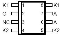
Package Cooled: SOP8
D/C: 06+


MFG:B(BOURNS) Package Cooled:SOP8 D/C:06+
TISP61511, TISP61511DR, TISP61512P Datasheet download
MFG: B(BOURNS)
Package Cooled: SOP8
D/C: 06+

Want to post a buying lead? If you are not a member yet, please select the specific/related part number first and then fill the quantity and your contact details in the "Request for Quotation Form" on the left, and then click "Send RFQ".Your buying lead can then be posted, and the reliable suppliers will quote via our online message system or other channels soon.
TOP
PDF/DataSheet Download
Datasheet: TISP61511D
File Size: 215060 KB
Manufacturer: POINN [Power Innovations Limited]
Download : Click here to Download
PDF/DataSheet Download
Datasheet: TIS150-124
File Size: 302333 KB
Manufacturer: TRACOPOWER [TRACO Electronic AG]
Download : Click here to Download
PDF/DataSheet Download
Datasheet: TISP61512P
File Size: 215060 KB
Manufacturer: POINN [Power Innovations Limited]
Download : Click here to Download
The TISP61511D and TISP61512P are dual forward-conducting buffered p-gate overvoltage protectors. They are designed to protect monolithic Subscriber Line Interface Circuits,SLICs, against overvoltages on the telephone line caused by lightning, ac power contact and induction. The TISP61511D and TISP61512P limit voltages that exceed the SLIC supply rail voltage.
The SLIC line driver section is typically poweredfrom 0 V (ground) and a negative voltage in the region of -10 V to -70 V. The protector gate is connected tothis negative supply. This references the protection (clipping) voltage to the negative supply voltage. As theprotection voltage will track the negative supply voltage the overvoltage stress on the SLIC is minimised.
Positive overvoltages are clipped to ground by diode forward conduction. Negative overvoltages are initially clipped close to the SLIC negative supply rail value. If sufficient current is available from the overvoltage, then the protector will crowbar into a low voltage on-state condition. As the current subsides the high holdingcurrent of the crowbar prevents d.c.latchup.
These monolithic protection devices are fabricated in ion-implanted planar vertical power structures for high reliability and in normal system operation they are virtually transparent. The buffered gate design reduces the loading on the SLIC supply during overvoltages caused by power cross and induction.
| RATING | SYMBOL | VALUE | UNIT |
| Repetitive peak off-state voltage, IG = 0, -40°C TJ85°C | VDRM | -100 | V |
| Repetitive peak gate-cathode voltage, VKA = 0, -40°C TJ 85°C | VGKRM | -85 | V |
| Non-repetitive peak on-state pulse current (see Notes 1 and 2) 10/1000 µs 5/310 µs 0.2/310 µs 1/20 µs 2/10 µs TJ = -40°C TJ = 25, 85°C |
ITSP | 30 40 40 90 120 170 |
A |
| Non-repetitive peak on-state current, 50 Hz (see Notes 1 and 2) full-sine-wave, 20 ms 1 s |
ITSM | 5 3.5 |
A |
| Non-repetitive peak gate current, half-sine-wave, 10 ms (see Notes 1and 2) | IGSM | 2 | A |
| Junction temperature | TJ | -55 to +150 | °C |
| Storage temperature range | Tstg | -55 to +150 | °C |

Price: 4-6 USD
MT58L64L18CT-10 TQFP100

Price: 5-6.5 USD
DL-7140-211M laser tube

Price: 4-5 USD
74LVC74APG - IC FLIP FLOP D-Type POS-EDG DUAL 14TSSOP

Price: 6.5-8 USD
CYPRESS - Clock Synthesizer with Differential CPU Outputs

Price: 0.284-0.286 USD
PI5V330QEX Pericom Multiplexer Switch ICs

Price: 1-2 USD
IGBT power module, Single switch, 1200 V, Collector-emitter voltage, 430A

Price: 1-2 USD
a-Si TFT-LCD, NEC, 228.096Hmm, 560V

Price: 0.124-0.2 USD
PC354N1T - Mini-flat Package, AC Input Type Photocoupler - Sharp Electrionic Components

Price: 0.177-0.178 USD
RL1210JR51-XX-BL - Thick Film Chip Resistor Low Ohmic - TAITRON Components Incorporated

Price: 0.053-0.055 USD
STPS140A - POWER SCHOTTKY RECTIFIER - STMicroelectronics

Price: 1.45-1.5 USD
STA013 - MPEG 2.5 LAYER III AUDIO DECODER - STMicroelectronics

Price: 0.073-0.075 USD
SMBJ5347B - 5 Watt Surface Mount Silicon Zener Diodes - Micro Commercial Components
