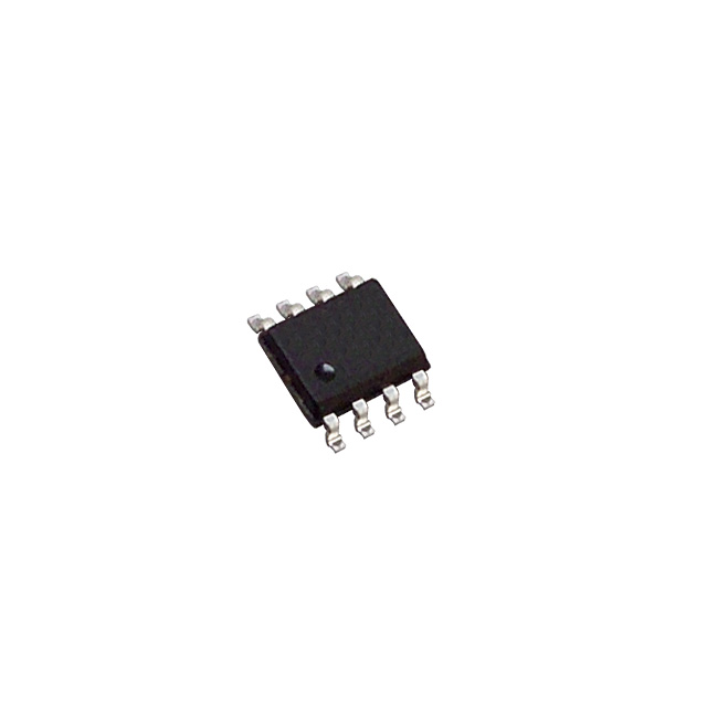
Want to post a buying lead? If you are not a member yet, please select the specific/related part number first and then fill the quantity and your contact details in the "Request for Quotation Form" on the left, and then click "Send RFQ".Your buying lead can then be posted, and the reliable suppliers will quote via our online message system or other channels soon.
The TL05x series of JFET-input operational amplifiers offers improved dc and ac characteristics over the TL07x and TL08x families of BiFET operational amplifiers. On-chip Zener trimming of offset voltage yields precision grades as low as 1.5 mV (TL051A) for greater accuracy in dc-coupled applications. Texas Instruments improved BiFET process and optimized designs also yield improved bandwidth and slew rate without increased power consumption. The TL05x devices are pin-compatible with the TL07x and TL08x and can be used to upgrade existing circuits or for optimal performance in new designs.
BiFET operational amplifiers offer the inherently higher input impedance of the JFET-input transistors, without sacrificing the output drive associated with bipolar amplifiers. This makes them better suited for interfacing with high-impedance sensors or very low-level ac signals. They also feature inherently better ac response than bipolar or CMOS devices having comparable power consumption.
The TL05x family was designed to offer higher precision and better ac response than the TL08x, with the low noise floor of the TL07x. Designers requiring significantly faster ac response or ensured lower noise should consider the Excalibur TLE208x and TLE207x families of BiFET operational amplifiers.
Because BiFET operational amplifiers are designed for use with dual power supplies, care must be taken to observe common-mode input voltage limits and output swing when operating from a single supply. DC biasing of the input signal is required, and loads should be terminated to a virtual-ground node at mid-supply. Texas Instruments TLE2426 integrated virtual ground generator is useful when operating BiFET amplifiers from single supplies.
The TL05x are fully specified at ±15 V and ±5 V. For operation in low-voltage and/or single-supply systems, Texas Instruments LinCMOS families of operational amplifiers (TLC-prefix) are recommended. When moving from BiFET to CMOS amplifiers, particular attention should be paid to the slew rate and bandwidth requirements, and also the output loading.
TL051 Maximum Ratings
Supply voltage, VCC+ (see Note 1). . . . . . . . . . .. . . . . . . . . . . . . .. . . . . . . . . . .18 V Supply voltage, VCC (see Note 1). . . . . . . . . . . .. . . . . . . . . . . . . .. . . . . . . . . 18 V Differential input voltage (see Note 2) . . . . . . . . . . . . . . . . . . . . . . . .. . . .. . . . ±30 V Input voltage range, VI (any input, see Notes 1 and 3) . . . . . . .. . . . . . . . . . . ±15 V Input current, II (each input) . . . . . . . . . .. . . . . . . . . . . . . .. . . . . . . . . . . . . . ±1 mA Output current, IO (each output) . . . . . . . . . . . . . . . . . . . . . .. . . . . . . . . . . . ±80 mA Total current into VCC+ . . . . . . . . . . . . . . . . . . . . . . . . . .. . . . . . . . . . . . . .. . 160 mA Total current out of VCC . . . . . . . . . . . . . . . . . . . . . . . .. . . . . . . . . . . . . . . . 160 mA Duration of short-circuit current at (or below) 25°C. . . . . . . . . . . .. . . . . . . Unlimited Package thermal impedance, JA (see Notes 4 and 5): D package (8 pin) . . 97°C/W D package (14 pin) . 86°C/W DB package (14 pin).96°C/W N package (14 pin) . 80°C/W NS package (14 pin).76°C/W P package (8 pin) . . 85°C/W PS package (8 pin) . 95°C/W Operating virtual junction temperature, TJ . . . . . . . . . . . . . . . . . . .. . . . . . . . .150°C Lead temperature 1,6 mm (1/16inch) from case for 10 seconds . . . . . . . . . . . 260°C Storage temperature range . . . . . . . . . .. . . . . . . . . .. . . . . . . . . .. . 65°C to 150°C † Stresses beyond those listed under "absolute maximum ratings" may cause permanent damage to the device. These are stress ratings only, and functional operation of the device at these or any other conditions beyond those indicated under "recommended operating conditions" is not implied. Exposure to absolute-maximum-rated conditions for extended periods may affect device reliability. NOTES: 1. All voltage values, except differential voltages, are with respect to the midpoint between VCC+ and VCC. 2. Differential voltages are at IN+ with respect to IN. 3. The magnitude of the input voltage must never exceed the magnitude of the supply voltage or 15 V, whichever is less. 4. Maximum power dissipation is a function of TJ(max), JA, and TA. The maximum allowable power dissipation at any allowable ambient temperature is PD = (TJ(max) TA)/JA. Operating at the absolute maximum TJ of 150°C can impact reliability. 5. The package thermal impedance is calculated in accordance with JESD 51-7.
The TL051ACP is designed as JFET-input operational amplifier which offers improved dc and ac characteristics over the TL07x and TL08x families of BiFET operational amplifiers. On-chip zener trimming of offset voltage yields precision grades as low as 1.5 mV (TL051A) for greater accuracy in dc-coupled applications. Its package is PDIP.
It has three features. (1)Direct upgrades to TL07x and TL08x BiFET operational amplifiers. (2)Faster slew rate (20 V/s typ) without increased power consumption. (3)On-chip offset-voltage trimming for improved DC performance and precision grades are available. That are all the main features.
Some absolute maximum ratings have been concluded into several points as follow. (1)Its supply voltage, Vcc+ would be 18V. (2)Its supply voltage, Vcc- is -18V. (3)Its differential input voltage would be +/-30V. (4)Its input voltage range (any input) would be +/-15V. (5)Its input current each input would be +/-1mA. (6)Its output current each output would be +/-80mA. (7)Its total curent in Vcc+ would be 160mA. (8)Its total current out of Vcc- would be 160mA. (8)Its duration of short-circuit at 25°C would be unlimited. (9)Its package thermal impedance would be 85°C/W for P package. (10)Its operating virtual junction temperature would be 150°C. (11)Its lead temperature 1,6mm (1/16 inch) from case for 10 seconds would be 260°C. (12)Its storage temperature range would be from -65°C to 150°C. It should be noted that stresses above those listed in absolute maximum ratings may cause permanent damage to device.
Also some electrical characteristics at Vcc=5V are concluded as follow. (1)Its input offset voltage would be typ 0.55mV and max 2.8mV at 25°C and would be max 3.8mV for full range. (2)Its temperature coefficient of input offset voltage would be typ 8uV/°C. (3)Its input offset voltage long term drift would be typ 0.04uV/mo. (4)Its input offset current would be typ 4pA and max 100pA at 25°C and would be typ 0.02nA and max 1nA at 70°C. And so on. If you have any question or suggestion or want to know more information please contact us for details. Thank you!