Want to post a buying lead? If you are not a member yet, please select the specific/related part number first and then fill the quantity and your contact details in the "Request for Quotation Form" on the left, and then click "Send RFQ".Your buying lead can then be posted, and the reliable suppliers will quote via our online message system or other channels soon.
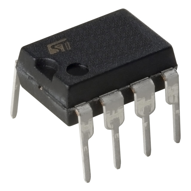
The TL061CP is designed as JFET-input operational amplifier which features high input impedance, wide bandwidth, high slew rate, and low input offset and input bias currents.
It has ten features. (1)Very low power consumption. (2)Typical supply current would be 200A (per amplifier). (3)Wide common-mode and differential voltage ranges. (4)Low input bias and offset currents. (5)Common-mode input voltage range includes VCC+. (6)Output short-circuit protection. (7)High input impedance JFET-input stage. (8)Internal frequency compensation. (9)Latch-up-free operation. (10)High slew rate which would be 3.5V/s typ. That are all the main features.
Some absolute maximum ratings have been concluded into several points as follow. (1)Its supply voltage Vcc+ would be 18V. (2)Its supply voltage Vcc- would be -18V. (3)Its differential input voltage would be +/-30V. (4)Its input voltage would be +/-15V. (5)Its duration of output short circuit would be unlimited. (6)Its package thermal impedance would be 85°C/W. (7)Its operatig virtual junction temperature would be 150°C. (8)Its lead temperature 1.6mm (1/16 inch) from case for 10 seconds would be 260°C. (9)Its storage temperature range would be from -65°C to 150°C. It should be noted that stresses above those listed in absolute maximum ratings may cause permanent damage to device.
Also some electrical characteristics are concluded as follow. (1)Its input offset voltage would be typ 3mV and max 15mV. (2)Its temperature coefficient of input offset voltage would be typ 10uV/°C. (3)Its input offset current would be typ 5pA and max 200pA. (4)Its input bias current would be typ 30pA and max 400pA. (5)Its common mode input voltage range would be min +/-11V and typ -12 to 15V. (6)Its maximum peak output voltage swing would be min +/-10V and typ +/-13.5V. (7)Its large signal differential voltage amplification would be min 3V/mV and typ 6V/mV. And so on. If you have any question or suggestion or want to know more information please contact us for details. Thank you!