Want to post a buying lead? If you are not a member yet, please select the specific/related part number first and then fill the quantity and your contact details in the "Request for Quotation Form" on the left, and then click "Send RFQ".Your buying lead can then be posted, and the reliable suppliers will quote via our online message system or other channels soon.
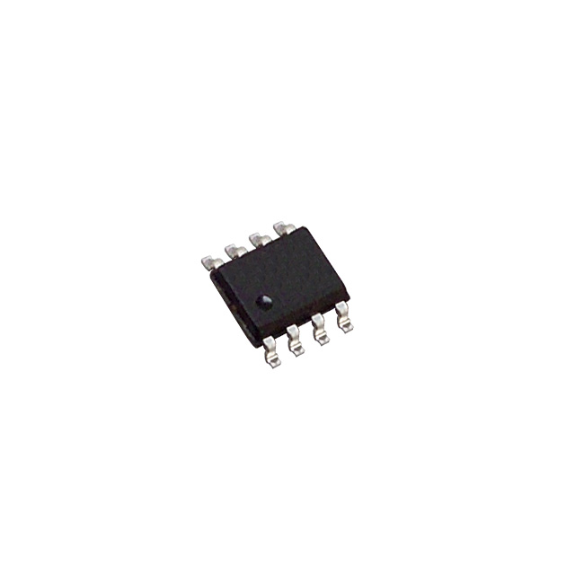
The TL7700 is a bipolar integrated circuit designed for use as a reset controller in microcomputer and microprocessor systems. The SENSE voltage can be set to any value greater than 0.5 V using two external resistors. The hysteresis value of the sense voltage also can be set by the same resistors. The device includes a precision voltage reference, fast comparator, timing generator, and output driver, so it can generate a power-on reset signal in a digital system.
The TL7700 has an internal 1.5-V temperature-compensated voltage reference from which all function blocks are supplied. Circuit function is very stable, with supply voltage in the 1.8-V to 40-V range. Minimum supply current allows use with ac line operation, portable battery operation, and automotive applications.
The TL7700C is characterized for operation from 40°C to 85°C.
TL7700 Maximum Ratings
Supply voltage, VCC (see Note 1) . . . . . . . . . . . . . . . . . . . . . . . . . . . .. . . . . . 41 V Sense input voltage range, Vs . . . . . . . . . . . . . . . . . . . . . . . . . . . .0.3 V to 41 V Output voltage, VOH (off state) . . . . . . . . . . . . . . . . . . . . . . . . . . . . . . . . . . . 41 V Output current, IOL (on state) . . . . . . . . . . . . . . . . . . . . . . . . . . . . . . . . . . . 5 mA Package thermal impedance, JA (see Notes 2 and 3): P package . . . . .. .85°C/W PS package . . . .. .95°C/W PW package . . . .149°C/W Storage temperature range, Tstg . . . . . . . . . . . . . . .. . . . . . . . . . 65°C to 150°C † Stresses beyond those listed under "absolute maximum ratings" may cause permanent damage to the device. These are stress ratings only, and functional operation of the device at these or any other conditions beyond those indicated under "recommended operating conditions" is not implied. Exposure to absolute-maximum-rated conditions for extended periods may affect device reliability. NOTES: 1. All voltage values are with respect to the network ground terminal. 2. Maximum power dissipation is a function of TJ(max), JA, and TA. The maximum allowable power dissipation at any allowable ambient temperature is PD = (TJ(max) TA)/JA. Operating at the absolute maximum TJ of 150°C can impact reliability. 3. The package thermal impedance is calculated in accordance with JESD 51.