TLP3012GB, TLP3020, TLP3021 Selling Leads, Datasheet
MFG:1000 Package Cooled:05+ D/C:08+09+

TLP3012GB, TLP3020, TLP3021 Datasheet download

Part Number: TLP3012GB
MFG: 1000
Package Cooled: 05+
D/C: 08+09+


MFG:1000 Package Cooled:05+ D/C:08+09+
TLP3012GB, TLP3020, TLP3021 Datasheet download
MFG: 1000
Package Cooled: 05+
D/C: 08+09+

Want to post a buying lead? If you are not a member yet, please select the specific/related part number first and then fill the quantity and your contact details in the "Request for Quotation Form" on the left, and then click "Send RFQ".Your buying lead can then be posted, and the reliable suppliers will quote via our online message system or other channels soon.
TOP
PDF/DataSheet Download
Datasheet: TLP
File Size: 345950 KB
Manufacturer: STMicroelectronics
Download : Click here to Download
PDF/DataSheet Download
Datasheet: TLP3020
File Size: 189065 KB
Manufacturer: TOSHIBA [Toshiba Semiconductor]
Download : Click here to Download
PDF/DataSheet Download
Datasheet: TLP3021
File Size: 189065 KB
Manufacturer: TOSHIBA [Toshiba Semiconductor]
Download : Click here to Download
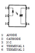
The TOSHIBA TLP3020, TLP3021, TLP3022 and TLP3023 consist of a photo-triac optically coupled to a gallium arsenide infrared emitting diode in a six lead plastic DIP package.
|
CHARACTERISTIC |
SYMBOL |
RATING |
UNIT | ||
|
LED |
Forward Current |
IF |
50 |
mA | |
| Forward Current Derating (Ta 53) |
IF/ |
−0.7 |
mA/ | ||
| Peak Forward Current (100s pulse, 100pps) |
IFP |
1 |
A | ||
| Power Dissipation |
PD |
100 |
mW | ||
| Power Dissipation Derating (Ta 25) |
PD/ |
−1.0 |
mW/ | ||
| Reverse Voltage |
VR |
5 |
V | ||
| Junction Temperature |
Tj |
125 |
|||
|
DETECTOR |
Off-State Output Terminal Voltage |
VDRM |
400 |
V | |
| On-Stage RMS | Ta=25 |
IT(RMS) |
100 |
mA | |
| Current | Ta=70 |
50 | |||
| On-State Current Derating (Ta 25) |
IT/ |
−1.1 |
mA/ | ||
| Peak On-Stage Current (100s pulse, 120pps) |
ITP |
2 |
A | ||
| Peak Nonrepetitive Surge Current (PW=10ms, DC=10%) |
ITSM |
1.2 |
A | ||
| Power Dissipation |
PD |
300 |
mW | ||
| Power Dissipation Derating (Ta 25) |
PD/ |
−4.0 |
mW/ | ||
| Junction Temperature |
Tj |
115 |
|||
| Storage Temperature Range |
Tstg |
−55 ~ 150 |
|||
| Operating Temperature Range |
Topr |
−40 ~ 100 |
|||
| Lead Soldering Temperature (10s) |
Tsol |
260 |
|||
| Total Package Power Dissipation |
PT |
330 |
mW | ||
| Total Package Power Dissipation Derating (Ta 25) |
PT/ |
−4.4 |
mW/ | ||
| Isolation Voltage (AC, 1 min., R.H. 60%) (Note 1) |
BVS |
5000 |
Vrms | ||
Note 1: Device considered a two terminal device :Pins 1, 2 and 3 shorted together and pins 4 and 6 shorted together.
Peak Off-State Voltage : 400 V (Min.)
Trigger LED Current : 30mA (Max.) (TLP3020)
15 mA (Max.) (TLP3021)
10 mA (Max.) (TLP3022)
5 mA (Max.) (TLP3023)
On-State Current : 100 mA (Max.)
UL Recognized : UL1577, File No. E67349
Isolation Voltage : 5000 Vrms (Min.)
Option (D4) Type
VDE Approved : DIN VDE0884 / 08.87,
Certificate No. 68329
Maximum Operating Insulation Voltage: 630 VPK
Highest Permissible Over Voltage: 6000 VPK
Note: When a VDE0884 approved type is needed, please designate the " Option (D4) "
7.62mm pich 10.16 mm pich
standard type (LF2) type
Creepage Distance : 7.0 mm (Min.) 8.0 mm (Min.)
Clearance : 7.0 mm (Min.) 8.0 mm (Min.)
Insulation Thickness : 0.5 mm (Min.) 0.5 mm (Min.)
|
CHARACTERISTIC |
SYMBOL |
RATING |
UNIT | ||
|
LED |
Forward Current |
IF |
50 |
mA | |
| Forward Current Derating (Ta 53) |
IF/ |
−0.7 |
mA/ | ||
| Peak Forward Current (100s pulse, 100pps) |
IFP |
1 |
A | ||
| Power Dissipation |
PD |
100 |
mW | ||
| Power Dissipation Derating (Ta 25) |
PD/ |
−1.0 |
mW/ | ||
| Reverse Voltage |
VR |
5 |
V | ||
| Junction Temperature |
Tj |
125 |
|||
|
DETECTOR |
Off-State Output Terminal Voltage |
VDRM |
400 |
V | |
| On-Stage RMS | Ta=25 |
IT(RMS) |
100 |
mA | |
| Current | Ta=70 |
50 | |||
| On-State Current Derating (Ta 25) |
IT/ |
−1.1 |
mA/ | ||
| Peak On-Stage Current (100s pulse, 120pps) |
ITP |
2 |
A | ||
| Peak Nonrepetitive Surge Current (PW=10ms, DC=10%) |
ITSM |
1.2 |
A | ||
| Power Dissipation |
PD |
300 |
mW | ||
| Power Dissipation Derating (Ta 25) |
PD/ |
−4.0 |
mW/ | ||
| Junction Temperature |
Tj |
115 |
|||
| Storage Temperature Range |
Tstg |
−55 ~ 150 |
|||
| Operating Temperature Range |
Topr |
−40 ~ 100 |
|||
| Lead Soldering Temperature (10s) |
Tsol |
260 |
|||
| Total Package Power Dissipation |
PT |
330 |
mW | ||
| Total Package Power Dissipation Derating (Ta 25) |
PT/ |
−4.4 |
mW/ | ||
| Isolation Voltage (AC, 1 min., R.H. 60%) (Note 1) |
BVS |
5000 |
Vrms | ||

Price: 4-6 USD
MT58L64L18CT-10 TQFP100

Price: 5-6.5 USD
DL-7140-211M laser tube

Price: 4-5 USD
74LVC74APG - IC FLIP FLOP D-Type POS-EDG DUAL 14TSSOP

Price: 6.5-8 USD
CYPRESS - Clock Synthesizer with Differential CPU Outputs

Price: 0.284-0.286 USD
PI5V330QEX Pericom Multiplexer Switch ICs

Price: 1-2 USD
IGBT power module, Single switch, 1200 V, Collector-emitter voltage, 430A

Price: 1-2 USD
a-Si TFT-LCD, NEC, 228.096Hmm, 560V

Price: 0.124-0.2 USD
PC354N1T - Mini-flat Package, AC Input Type Photocoupler - Sharp Electrionic Components

Price: 0.177-0.178 USD
RL1210JR51-XX-BL - Thick Film Chip Resistor Low Ohmic - TAITRON Components Incorporated

Price: 0.053-0.055 USD
STPS140A - POWER SCHOTTKY RECTIFIER - STMicroelectronics

Price: 1.45-1.5 USD
STA013 - MPEG 2.5 LAYER III AUDIO DECODER - STMicroelectronics

Price: 0.073-0.075 USD
SMBJ5347B - 5 Watt Surface Mount Silicon Zener Diodes - Micro Commercial Components
