Want to post a buying lead? If you are not a member yet, please select the specific/related part number first and then fill the quantity and your contact details in the "Request for Quotation Form" on the left, and then click "Send RFQ".Your buying lead can then be posted, and the reliable suppliers will quote via our online message system or other channels soon.
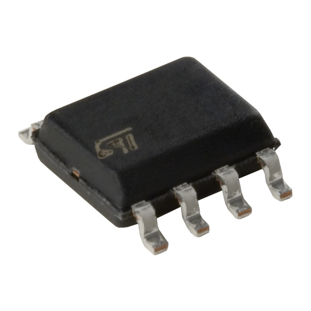
These devices consist of two independent preci- sion voltage comparators, designed to operate with single or dual supplies.
These differential comparators use the STMicro-electronics silicon lin MOS process giving them an excellent consumption-speed ratio.
These devices are ideally suited for low consump-tion applications.
TS372 Maximum Ratings
Symbol
Parameter
Value
Unit
VCC+
Supply Voltage 1)
18
V
Vid
Differential Input Voltage 2)
±18
V
Vi
Input Voltage 3)
18
V
Vo
Output Voltage
18
V
Io
Output Current
20
mA
IF
Forward Current in ESD Protection Diodes onInput 4)
50
mA
Duration of Output-Circuit to GND 5)
Infinite
pd
Power Dissipation 6) DIP8 SO8
1250 710
mW
Tstg
Storage Temperature Range
-65 to +150
Tj
Junction Temperature
+150
1. All voltage values, except differential voltage, are with respect to network ground terminal. 2. Differential voltages are the non-inverting input terminal with respect to the inverting input terminal. 3. The magnitude of the input and the output voltages must never exceed the magnitude of the possitive supply voltage. 4. Guaranteed by design. 5. Short circuit from outputs to Vcc+ can cause excessive heating and eventual destruction. 6. Pd is calculated with Tamb = +25°C, Tj = +150°C and Rthja = 100°C/W for DIP8 package = 175°C/W for SO8 package
TS372 Features
· WIDE SINGLE SUPPLY RANGE OR DUAL SUPPLIES 3V TO 16V OR ±1.5V TO ±8V · VERY LOW SUPPLY CURRENT: 0.1mA/COMP INDEPENDENT OF SUPPLY VOLTAGE · EXTREMELY LOW INPUT BIAS CURRENT :1pA typ · EXTREMELY LOW INPUT OFFSET CURRENTS : 1pA typ · LOW INPUT OFFSET VOLTAGE · INPUT COMMON-MODE VOLTAGE RANGE INCLUDES GND · LOW OUTPUT SATURATION VOLTAGE 150mV TYP · OUTPUT COMPATIBLE WITH TTL, MOS AND CMOS · HIGH INPUT IMPEDANCE : 1012Ω typ · FAST RESPONSE TIME : 200ns TYP FOR TTL LEVEL INPUT STEP