Want to post a buying lead? If you are not a member yet, please select the specific/related part number first and then fill the quantity and your contact details in the "Request for Quotation Form" on the left, and then click "Send RFQ".Your buying lead can then be posted, and the reliable suppliers will quote via our online message system or other channels soon.
These N-Channel enhancement mode power field effect transistors are produced using Fairchild's proprietary, planar stripe,DMOS technology.
This advanced technology has been especially tailored to minimize on-state resistance, provide superior switching performance, and withstand high energy pulse in the avalanche and commutation mode. These devices are well suited for high efficient switched mode power supplies and active power factor correction.
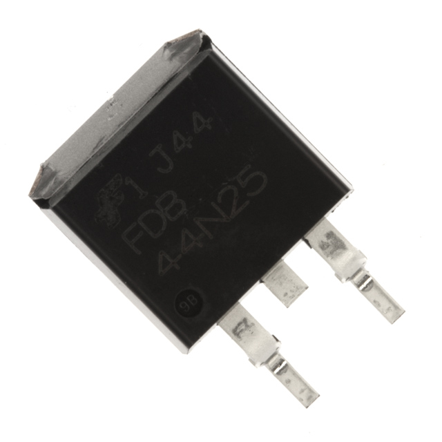
FDB44N25 Maximum Ratings
Symbol
Parameter
FDB44N25
Units
VDSS
Drain-Source Voltage
250
V
ID
Drain Current - Continuous (TC = 25°C)
- Continuous (TC = 100°C)
44
A
26.4
A
IDM
Drain Current - Pulsed (Note 1)
176
A
VGSS
Gate-Source Voltage
± 30
V
EAS
Single Pulsed Avalanche Energy (Note 2)
2055
mJ
IAR
Avalanche Current (Note 1)
44
A
EAR
Repetitive Avalanche Energy (Note 1)
30.7
mJ
dv/dt
Peak Diode Recovery dv/dt (Note 3)
4.5
V/ns
PD
Power Dissipation (TC = 25°C) - Derate above 25°C
307
2.45
W
W/°C
TJ, TSTG
Operating and Storage Temperature Range
-55 to +150
°C
TL
Maximum lead temperature for soldering purposes,1/8" from case for 5 seconds
These N-Channel enhancement mode power field effect transis-tors are produced using Fairchild's proprietary, planar stripe,DMOS technology.
This advanced technology has been especially tailored to mini-mize on-state resistance, provide superior switching perfor-mance, and withstand high energy pulse in the avalanche and commutation mode. These devices are well suited for high effi-cient switched mode power supplies and active power factor correction.