Want to post a buying lead? If you are not a member yet, please select the specific/related part number first and then fill the quantity and your contact details in the "Request for Quotation Form" on the left, and then click "Send RFQ".Your buying lead can then be posted, and the reliable suppliers will quote via our online message system or other channels soon.
This device is particularly suited for compact power management. In portable electronic equipment where 2.5V to 6V input capability is needed. This load switch integrates a Slew Rate Control Driver that drives a P-Channel Power MOSFET in one tiny SuperSOT-6 package. The integrated slew rate control driver is specifically designed to control the turn on of the P-Channel MOSFET in order to limit the inrush current in battery switching applications with high capacitance loads. For turn-off, the IC pulls the MOSFET gate up quickly.
FDC6901L Maximum Ratings
Symbol
Parameter
Ratings
Units
VDD
Supply Voltage
0.5 to 10
V
VIN
DC Input Voltage (Logic Inputs)
0.7 to 6
V
PD
Power Dissipation
TSTG
Storage Junction Temperature Range
55 to +150
°C
FDC6901L Features
• Three programmable slew rates • Reduces inrush current • Minimizes EMI • Normal turn-off speed • Low-power CMOS operates over wide voltage range • High performance trench technology for extremely low RDS(ON)
FDC6901L Typical Application
• Load switch • Power management
FDC697P Parameters
Technical/Catalog Information
FDC697P
Vendor
Fairchild Semiconductor
Category
Discrete Semiconductor Products
Mounting Type
Surface Mount
FET Polarity
P-Channel
Drain to Source Voltage (Vdss)
20V
Current - Continuous Drain (Id) @ 25° C
8A
Rds On (Max) @ Id, Vgs
20 mOhm @ 8A, 4.5V
Input Capacitance (Ciss) @ Vds
3524pF @ 10V
Power - Max
1.5W
Packaging
Tape & Reel (TR)
Gate Charge (Qg) @ Vgs
55nC @ 4.5V
Package / Case
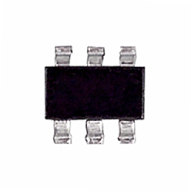
SuperSOT-6
FET Feature
Logic Level Gate
Drawing Number
*
Lead Free Status
Lead Free
RoHS Status
RoHS Compliant
Other Names
FDC697P FDC697P
FDC697P General Description
This P-Channel 1.8V specified MOSFET uses Fairchild's advanced low voltage Power Trench process. It has been optimized for battery power management applications.
FDC697P Maximum Ratings
Symbol
Parameter
Ratings
Units
VDSS
Drain-Source Voltage
20
V
VGSS
Gate-Source Voltage
±8
V
ID
Drain Current Continuous (Note 1a)
Pulsed
-8
A
-40
PD
Maximum Power Dissipation (Note 1a)
(Note 1b)
2
W
1.5
TJ, TSTG
Operating and Storage Junction Temperature Range
-55 to +150
FDC697P Features
8 A, 20 V RDS(ON) = 20 m @ VGS = 4.5 V RDS(ON) = 25 m @ VGS = 2.5 V RDS(ON) = 35 m @ VGS = 1.8 V High performance trench technology for extremely low RDS(ON) Fast switching speed FLMP SuperSOT-6 package: Enhanced thermal performance in industry-standard package size
This P-Channel 2.5V specified MOSFET is a rugged gate version of Fairchild Semiconductor's advanced PowerTrench process. It has been optimized for power management applications with a wide range of gate drive voltage (2.5V 12V).
FDC699P Maximum Ratings
Symbol
Parameter
Ratings
Units
VDSS
Drain-Source Voltage
12
V
VGSS
Gate-Source Voltage
±12
V
ID
Drain Current Continuous (Note 1a)
Pulsed
-7
A
-40
PD
Maximum Power Dissipation (Note 1a)
(Note 1b)
2
W
1.5
TJ, TSTG
Operating and Storage Junction Temperature Range
-55 to +150
FDC699P Features
7 A, 20 V RDS(ON) = 22 m @ VGS = 4.5 V RDS(ON) = 30 m@ VGS = 2.5 V High performance trench technology for extremely low RDS(ON) Fast switching speed FLMP SuperSOT-6 package: Enhanced thermal performance in industry-standard package size