Want to post a buying lead? If you are not a member yet, please select the specific/related part number first and then fill the quantity and your contact details in the "Request for Quotation Form" on the left, and then click "Send RFQ".Your buying lead can then be posted, and the reliable suppliers will quote via our online message system or other channels soon.
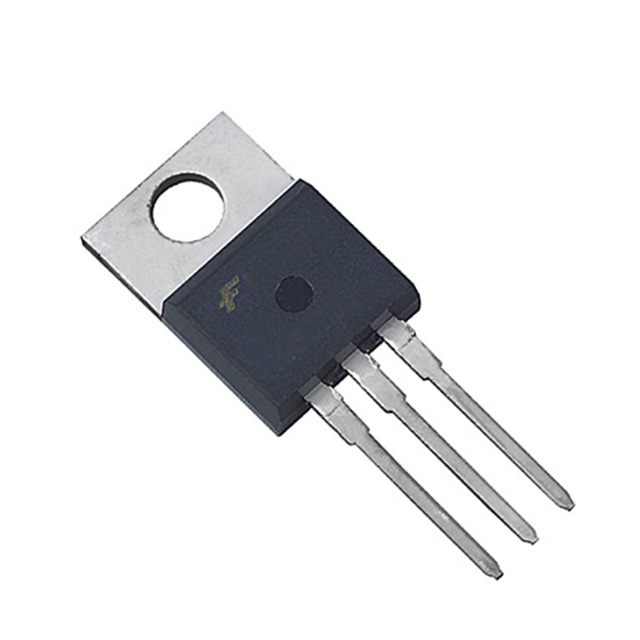
These are N-Channel enhancement mode silicon gate power field effect transistors. They are advanced power MOSFETs designed, tested, and guaranteed to withstand a specified level of energy in the breakdown avalanche mode of operation. All of these power MOSFETs are designed for applications such as switching regulators, switching converters, motor drivers, relay drivers, and drivers for high power bipolar switching transistors requiring high speed and low gate drive power. These types can be operated directly from integrated circuits.
HRF3205 Maximum Ratings
Drain to Source Voltage (Note 1)
VDSS
55
V
Drain to Gate Voltage (RGS = 20kW) (Note 1)
VDGR
55
V
Gate to Source Voltage
VGS
±20V
V
Drain Current Drain Current
ID
100
A
Drain Current Pulsed Drain Current (Note 2)
IDM
390
A
Pulsed Avalanche Rating
EAS
Figure 10
Power Dissipation
PD
175
W
Derate Above 25oC
1.17
W/
Operating and Storage Temperature
TJ,TSTG
-55 to 175
Maximum Temperature for Soldering
Leads at 0.063in (1.6mm) from Case for 10s.
TL
300
Package Body for 10s, See Techbrief 334
Tpkg
260
HRF3205 Features
• 100A, 55V (See Note) • Low On-Resistance, rDS(ON) = 0.008W • Temperature Compensating PSPICE® Model • Thermal Impedance SPICE Model • UIS Rating Curve • Related Literature - TB334, "Guidelines for Soldering Surface Mount Components to PC Boards"