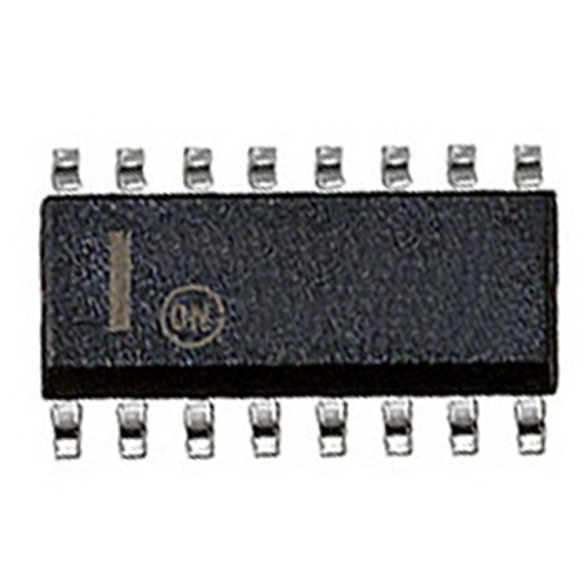
Description
The MC26LS30 is a dual function line driver it can be configured as two differential output drivers which comply with EIA422A Standard, or as four singleended drivers which comply with EIA423A Standard. The mode of operation is selected with the Mode pin (Pin 4) and appropriate power supplies (see Table 1). Each of the four outputs is capable of sourcing and sinking 60 to 70 mA while providing sufficient voltage to ensure proper data transmission.
As differential drivers, data rates to 10 Mbaud can be transmitted over a twisted pair for a distance determined by the cable characteristics. EIA422A Standard provides guidelines for cable length versus data rate. The advantage of a differential (balanced) system over a singleended system is greater noise immunity, common mode rejection,
and higher data rates.
Where extraneous noise sources are not a problem, the MC26LS30 may be configured as four singleended drivers transmitting data rates to 100 Kbaud. Crosstalk among wires within a cable is controlled by the use of the slew rate control pins on the MC26LS30.
Mode Selection (Differential Mode)
In this mode (Pins 4 and 8 at ground), only a +5.0 V supply ±5% is required at VCC. Pins 2 and 7 are the driver inputs, while Pins 10, 11, 14 and 15 are the outputs (see Block Diagram on page 1). The two outputs of a driver are always complementary and the differential voltage available at each pair of outputs is shown in Figure 6 for VCC = 5.0 V. The differential output voltage will vary directly with VCC. A "high" output can only source current, while a "low" output can only sink current (except for short circuit current see Figure 8).
The two outputs will be in a high impedance mode when the respective Enable input (Pin 3 or 6) is high, or if VCC
1.1 V. Output leakage current over a common mode range of ± 10 V is typically less than 1.0 A.
The outputs have short circuit current limiting, typically, less than 100 mA over a voltage range of 0 to +6.0 V (see Figure 8). Short circuits should not be allowed to last indefinitely as the IC may be damaged.
Pins 9, 12, 13 and 16 are not normally used when in this mode, and should be left open.
(SingleEnded Mode)
In this mode (Pin 4 2.0 V) VCC requires +5.0 V, and VEE requires 5.0 V, both ±5.0%. Pins 2, 3, 6, and 7 are inputs for the four drivers, and Pins 15, 14, 11, and 10 (respectively) are the outputs. The four drivers are independent of each other, and each output will be at a positive or a negative voltage depending on its input state, the load current, and the supply voltage. Figures 10 & 11 indicate the high and low output voltages for VCC = 5.0 V, and VEE = 5.0 V. The graph of Figure 10 will vary directly with VCC, and the graph of Figure 11 will vary directly with VEE. A "high" output can only source current, while a "low" output can only sink current (except short circuit current see Figure 14).
The outputs will be in a high impedance mode only if VCC 1.1 V. Changing VEE to 0 V does not set the outputs to a high impedance mode. Leakage current over a common mode range of ±10 V is typically less than 1.0 A.
The outputs have short circuit current limiting, typically less than 100 mA over a voltage range of ±6.0 V (see Figure
14). Short circuits should not be allowed to last indefinitely as the IC may be damaged.
Capacitors connected between Pins 9, 12, 13, and 16 and their respective outputs will provide slew rate limiting of the output transition. Figure 16 indicates the required capacitor value to obtain a desired rise or fall time (measured between the 10% and 90% points). The positive and negative transition times will be within ±5% of each other. Each output may be set to a different slew rate if desired.
Inputs
The five inputs determine the state of the outputs in accordance with Table 1. All inputs (regardless of the operating mode) have a nominal threshold of +1.3 V, and their voltage must be kept within a range of 0 V to +15 V for
proper operation. If an input is taken more than 0.3 V below ground, excessive currents will flow, and the proper
operation of the drivers will be affected. An open pin is equivalent to a logic high, but good design practices dictate
that inputs should never be left open. Unused inputs should be connected to ground. The characteristics of the inputs are shown in Figure 9.
Power Supplies
VCC requires +5.0 V, ±5%, regardless of the mode of operation. The supply current is determined by the IC's internal bias requirements and the total load current. The internally required current is a function of the load current
and is shown in Figure 7 for the differential mode.
In the singleended mode, VEE must be 5.0 V, ±5% in order to comply with EIA423A standards. Figures 12 and
13 indicate the internally required bias currents as a function of total load current (the sum of the four output loads). The discontinuity at 0 load current exists due to a change in bias current when the inputs are switched. The supply currents vary ± 2.0 mA as VCC and VEE are varied from |4.75 V| to |5.25 V|.
Sequencing of the supplies during powerup/ powerdown is not required.
Bypass capacitors (0.1 mF minimum on each supply pin) are recommended to ensure proper operation. Capacitors reduce noise induced onto the supply lines by the switching action of the drivers, particularly where long P.C. board
tracks are involved. Additionally, the capacitors help absorb transients induced onto the drivers' outputs from the external cable (from ESD, motor noise, nearby computers, etc.).
Operating Temperature Range
The maximum ambient operating temperature, listed as +85, is actually a function of the system use (i.e., specifically how many drivers within a package are used) and at what current levels they are operating. The maximum power which may be dissipated within the package is determined by:
PDmax = TJmax-TA
RJA
where RqJA = package thermal resistance which is typically:
120/W for the SOIC (D) package,
TJmax = max. allowable junction temperature (150°C)
TA = ambient air temperature near the IC package.
1) Differential Mode Power Dissipation
For the differential mode, the power dissipated within the package is calculated from:
PD = [ (VCC- VOD)* IO ] (each driver)+(VCC* IB)
where: VCC = the supply voltage
VOD = is taken from Figure 6 for the known value of IO
IB = the internal bias current (Figure 7)
As indicated in the equation, the first term (in brackets) must be calculated and summed for each of the two drivers, while the last term is common to the entire package. Note that the term (VCC VOD) is constant for a given value of IO and does not vary with VCC. For an application involving the following conditions:
TA = +85, IO = 60 mA (each driver), VCC = 5.25 V, the suitability of the package types is calculated as follows.
The power dissipated is:
PD = [ 3.0 V*60 mA*2 ]+(5.25 V*18 mA)
PD = 454 mW
The junction temperature calculates to:
TJ =85+(0.454 W*120/W)=139 for the SOIC package.
Since the maximum allowable junction temperature is not exceeded in any of the above cases, either package can be used in this application.
2) SingleEnded Mode Power Dissipation
For the singleended mode, the power dissipated within the package is calculated from:
PD = (IB+*VCC)+(IB-*VEE)+ [ (IO*(VCC-VOH) ] (each driver)
The above equation assumes IO has the same magnitude for both output states, and makes use of the fact that the
absolute value of the graphs of Figures 10 and 11 are nearly identical. IB+ and IB are obtained from the right half of Figures 12 and 13, and (VCC VOH) can be obtained from Figure 10. Note that the term (VCC VOH) is constant for a given value of IO and does not vary with VCC. For an application involving the following conditions:
TA = +85, IO = 60 mA (each driver), VCC = 5.25 V, VEE = 5.25 V, the suitability of the package types is calculated as follows.
The power dissipated is:
PD = (24 mA*5.25 V)+(-3.0 mA*-5.25 V)+ [ 60 mA*1.45 V* 4.0 ]
PD =490 mW
The junction temperature calculates to:
TJ = 85+(0.490 W*120/W) =144 for the SOIC package.
Since the maximum allowable junction temperature is not exceeded in any of the above cases, either package can be used in this application.