Want to post a buying lead? If you are not a member yet, please select the specific/related part number first and then fill the quantity and your contact details in the "Request for Quotation Form" on the left, and then click "Send RFQ".Your buying lead can then be posted, and the reliable suppliers will quote via our online message system or other channels soon.
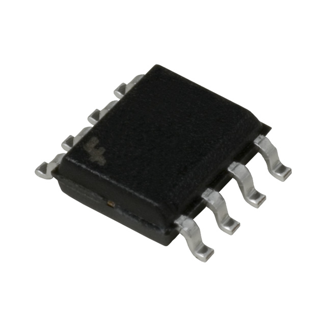
These devices consist of a gallium arsenide infrared emitting diode optically coupled to a monolithic silicon phototransistor detector, in a surface mountable, small outline, plastic package. They are ideally suited for high density applications, and eliminate the need for throughtheboard mounting.
MOC215 Maximum Ratings
Rating
Symbol
Value
Unit
INPUT LED
Forward Current - Continuous
IF
60
mA
Forward Current - Peak (PW = 100 s, 120 pps)
IF(pk)
1.0
A
Reverse Voltage
VR
6.0
V
LED Power Dissipation @ TA = 25 Derate above 25
PD
90 0.8
mW mW/
OUTPUT DARLINGTON
CollectorEmitter Voltage
VCEO
30
V
CollectorBase Voltage
VCBO
70
V
EmitterCollector Voltage
VECO
7.0
V
Collector Current - Continuous
IC
150
mA
Detector Power Dissipation @ TA = 25 Derate above 25
PD
150 1.76
mW mW/
TOTAL DEVICE
InputOutput Isolation Voltage(1,2) (60 Hz, 1.0 sec. duration)
VISO
3000
Vac(rms)
Total Device Power Dissipation @ TA = 25 Derate above 25
PD
250 2.94
mW mW/
Ambient Operating Temperature Range(3)
TA
55 to +100
Storage Temperature Range(3)
Tstg
55 to +150
Lead Soldering Temperature (1/16" from case, 10 sec. duration)
-
260
NOTE: Thickness through insulation between input and output is 0.5 mm.
MOC215 Features
• Convenient Plastic SOIC8 Surface Mountable Package Style • Low LED Input Current Required, for Easier Logic Interfacing • Standard SOIC8 Footprint, with 0.050, Lead Spacing • Shipped in Tape and Reel, which Conforms to EIA Standard RS481A • Compatible with Dual Wave, Vapor Phase and IR Reflow Soldering • High InputOutput Isolation of 3000 Vac (rms) Guaranteed • UL Recognized File #E54915
MOC215 Typical Application
• Low power Logic Circuits • Interfacing and coupling systems of different potentials and impedances • Telecommunications equipment • Portable electronics
MOC216 General Description
These devices consist of a gallium arsenide infrared emitting diode optically coupled to a monolithic silicon phototransistor detector, in a surface mountable, small outline, plastic package. They are ideally suited for high density applications, and eliminate the need for throughtheboard mounting.
MOC216 Maximum Ratings
Rating
Symbol
Value
Unit
INPUT LED
Forward Current - Continuous
IF
60
mA
Forward Current - Peak (PW = 100 s, 120 pps)
IF(pk)
1.0
A
Reverse Voltage
VR
6.0
V
LED Power Dissipation @ TA = 25 Derate above 25
PD
90 0.8
mW mW/
OUTPUT DARLINGTON
CollectorEmitter Voltage
VCEO
30
V
CollectorBase Voltage
VCBO
70
V
EmitterCollector Voltage
VECO
7.0
V
Collector Current - Continuous
IC
150
mA
Detector Power Dissipation @ TA = 25 Derate above 25
PD
150 1.76
mW mW/
TOTAL DEVICE
InputOutput Isolation Voltage(1,2) (60 Hz, 1.0 sec. duration)
VISO
3000
Vac(rms)
Total Device Power Dissipation @ TA = 25 Derate above 25
PD
250 2.94
mW mW/
Ambient Operating Temperature Range(3)
TA
55 to +100
Storage Temperature Range(3)
Tstg
55 to +150
Lead Soldering Temperature (1/16" from case, 10 sec. duration)
-
260
NOTE: Thickness through insulation between input and output is 0.5 mm.
MOC216 Features
• Convenient Plastic SOIC8 Surface Mountable Package Style • Low LED Input Current Required, for Easier Logic Interfacing • Standard SOIC8 Footprint, with 0.050, Lead Spacing • Shipped in Tape and Reel, which Conforms to EIA Standard RS481A • Compatible with Dual Wave, Vapor Phase and IR Reflow Soldering • High InputOutput Isolation of 3000 Vac (rms) Guaranteed • UL Recognized File #E54915
MOC216 Typical Application
• Low power Logic Circuits • Interfacing and coupling systems of different potentials and impedances • Telecommunications equipment • Portable electronics