Want to post a buying lead? If you are not a member yet, please select the specific/related part number first and then fill the quantity and your contact details in the "Request for Quotation Form" on the left, and then click "Send RFQ".Your buying lead can then be posted, and the reliable suppliers will quote via our online message system or other channels soon.
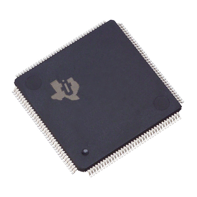
The Texas Instruments PCI2050 PCI-to-PCI bridge provides a high performance connection path between two peripheral component interconnect (PCI) buses. Transactions occur between masters on one PCI bus and targets on another PCI bus, and the PCI2050 allows bridged transactions to occur concurrently on both buses. The bridge supports burst-mode transfers to maximize data throughput, and the two bus traffic paths through the bridge act independently.
The PCI2050 bridge is compliant with the PCI Local Bus Specification, and can be used to overcome the electrical loading limits of 10 devices per PCI bus and one PCI device per expansion slot by creating hierarchical buses. The PCI2050 provides two-tier internal arbitration for up to nine secondary bus masters and may be implemented with an external secondary PCI bus arbiter.
The compact-PCI hot-swap extended PCI capability is provided which makes the PCI2050 an ideal solution for multifunction compact PCI cards and adapting single function cards to hot-swap compliance.
The PCI2050 bridge is compliant with the PCI-to-PCI Bridge Specification 1.1. The PCI 2050 provides compliance for PCI Power Management 1.0 and 1.1. The PCI2050 has been designed to lead the industry in power conservation. An advanced CMOS process is used to achieve low system power consumption while operating at PCI clock rates up to 33 MHz.
PCI2050 Maximum Ratings
Supply voltage range: VCC . . . . . . . . . . . . . . . . . . . . . . . . . 0.5 V to 3.6 V : S_VCCP . . . . . . . . . . . . . . . . . . 0.5 V to 6 V : P_VCCP . . . . . . . . . . . . . . . . . . . 0.5 V to 6 V Input voltage range, VI: PCI . . . . . . . . . . . . . . . . . . . . . . 0.5 V to 6.5 V Output voltage range, VO: PCI . . . . . . . . . . . . . . . . . 0.5 V to VCC + 0.5 V Input clamp current, IIK (VI < 0 or VI > VCC) (see Note 1) . . . . . . . ±20 mA Output clamp current, IOK (VO < 0 or VO > VCC) (see Note 2) . . . . . ±20 mA Storage temperature range, Tstg . . . . . . . . . . . . . . . . . . . . .65°C to 150°C Virtual junction temperature, TJ . . . . . . . . . . . . . . . . . . . . . . . . . . . 150°C
PCI2050 Features
• Configurable for PCI Bus Power Management Interface Specification • Provides compact PCI hot-swap functionality • 3.3-V core logic with universal PCI interfaces compatible with 3.3-V and 5-V PCI signaling environments • Two 32-bit, 33-MHz PCI buses • Provides internal two-tier arbitration for up to nine secondary bus masters and supports an external secondary bus arbiter • Burst data transfers with pipeline architecture to maximize data throughput in both directions • Independent read and write buffers for each direction • Up to three delayed transactions in both directions • Provides 10 secondary PCI clock outputs • Predictable latency per PCI Local Bus Specification • Propagates bus locking • Secondary bus is driven low during reset • Provides VGA/palette memory and I/O, and subtractive decoding options • Advanced submicron, low-power CMOS technology • Packaged in 208-terminal QFP or 209-terminal MicroStar BGA